M30833FJFP#U5 Renesas Electronics America, M30833FJFP#U5 Datasheet - Page 408
M30833FJFP#U5
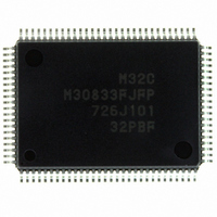
Manufacturer Part Number
M30833FJFP#U5
Description
IC M32C/83 MCU FLASH 100QFP
Manufacturer
Renesas Electronics America
Series
M16C™ M32C/80r
Datasheets
1.M3087BFLGPU3.pdf
(364 pages)
2.M30833FJGPU3.pdf
(96 pages)
3.M30833FJGPU3.pdf
(529 pages)
Specifications of M30833FJFP#U5
Core Processor
M32C/80
Core Size
16/32-Bit
Speed
32MHz
Connectivity
CAN, I²C, IEBus, SIO, UART/USART
Peripherals
DMA, WDT
Number Of I /o
85
Program Memory Size
512KB (512K x 8)
Program Memory Type
FLASH
Ram Size
31K x 8
Voltage - Supply (vcc/vdd)
3 V ~ 5.5 V
Data Converters
A/D 26x10b; D/A 2x8b
Oscillator Type
Internal
Operating Temperature
-20°C ~ 85°C
Package / Case
100-QFP
For Use With
R0K330879S001BE - KIT DEV RSK M32C/87R0K330879S000BE - KIT DEV RSK M32C/87
Lead Free Status / RoHS Status
Lead free / RoHS Compliant
Eeprom Size
-
Available stocks
Company
Part Number
Manufacturer
Quantity
Price

Part Number:
M30833FJFP#U5M30833FJFP#U3
Manufacturer:
Renesas Electronics America
Quantity:
135
Part Number:
M30833FJFP#U5M30833FJFP#U3
Manufacturer:
Renesas Electronics America
Quantity:
10 000


R
R
M
e
E
3
. v
J
Figure 24.18 IPS Register
2
Figure 23.17 PCR Register
0
1
C
9
3 .
B
8 /
0
1
3
0
3
J
G
4
Input Function Select Register
a
Port Control Register
b7
b7
0 -
n
o r
3 .
1
u
b6
b6
, 1
3
NOTES:
p
NOTES:
1
2
b5
(
b5
1. Although AN15
M
1. Set the PUR0 bit to "0" since P1 operates as the data bus in memory expansion mode and
2. This function is designed, not to make port P1 a full open drain, but to turn off the P channel in the
0
0
increase.
3
microprocessor mode. When using the ports as I/O ports, CMOS port or N-channel open drain
can be selected.
b4
CMOS port.Absolute maximum rating of the input voltage is from -0.3V to V
b4
6
2
C
b3
b3
Page 383
8 /
b2
, 3
b2
M
b1
b1
3
b0
2
b0
0
C
to AN15
f o
8 /
(b7 - b1)
Symbol
Symbol
4
PCR0
IPS0
IPS1
IPS2
IPS3
IPS4
IPS5
IPS6
IPS7
3
8
Bit
Bit
) T
(1)
8
Symbol
IPS
Symbol
PCR
7
can be used when the IPS bit is set to "0", the power consumption may
Group 0 Input Pin
Select Bit 0
Group 1 Input Pin
Select Bit 1
Port P15 Input Peripheral
Function Select Bit
CAN
Pin Select Bit
ISRxD2/IE
Pin Select Bit
ISCLK2 Function
Pin Select Bit
ISRxD3 Function
Pin Select Bit
Port P1 Control
Bit
Nothing is assigned. When write, set to "0".
When read, its content is indeterminate.
IN
Bit Name
Function
Bit Name
IN
Address
0178
Address
03FF
Function
16
16
0 : CMOS output as P1 output format
1 : N-channel open drain output
b5
Assigns each function of INPC0
INPC0
/BE0
0 : P7
1 : P15
Assigns each function of INPC1
/ISCLK1 and INPC1
to the following ports.
0 : P7
1 : P11
0 : Except AN15
1 : AN15
0 : P7
1 : P8
0 : P6
1 : P13
0 : P8
1 : P12
0
0
1
1
b4
0
1
0
1
IN
: P7
: P9
: P13
: Do not set to this value
6,
4,
7
3
4
1,
1
1,
to the following ports.
0,
6
0,
/ISCLK0 and INPC0
P7
P7
P8
P11
P15
P12
1
1
7,
5
5
2
P8
After Reset
00
2
After Reset
XXXX XXX0
1,
2
Function
Function
16
P15
0
(1)
2
2
/ISRxD1/BE1
CC
+ 0.3V.
2
24. Programmable I/O Port
(2)
2
/ISRxD0
0
1
,
IN
RW
RW
RW
RW
RW
RW
RW
RW
RW
RW
RW
Related parts for M30833FJFP#U5
Image
Part Number
Description
Manufacturer
Datasheet
Request
R

Part Number:
Description:
KIT STARTER FOR M16C/29
Manufacturer:
Renesas Electronics America
Datasheet:

Part Number:
Description:
KIT STARTER FOR R8C/2D
Manufacturer:
Renesas Electronics America
Datasheet:

Part Number:
Description:
R0K33062P STARTER KIT
Manufacturer:
Renesas Electronics America
Datasheet:

Part Number:
Description:
KIT STARTER FOR R8C/23 E8A
Manufacturer:
Renesas Electronics America
Datasheet:

Part Number:
Description:
KIT STARTER FOR R8C/25
Manufacturer:
Renesas Electronics America
Datasheet:

Part Number:
Description:
KIT STARTER H8S2456 SHARPE DSPLY
Manufacturer:
Renesas Electronics America
Datasheet:

Part Number:
Description:
KIT STARTER FOR R8C38C
Manufacturer:
Renesas Electronics America
Datasheet:

Part Number:
Description:
KIT STARTER FOR R8C35C
Manufacturer:
Renesas Electronics America
Datasheet:

Part Number:
Description:
KIT STARTER FOR R8CL3AC+LCD APPS
Manufacturer:
Renesas Electronics America
Datasheet:
Part Number:
Description:
KIT STARTER FOR RX610
Manufacturer:
Renesas Electronics America
Datasheet:

Part Number:
Description:
KIT STARTER FOR R32C/118
Manufacturer:
Renesas Electronics America
Datasheet:

Part Number:
Description:
KIT DEV RSK-R8C/26-29
Manufacturer:
Renesas Electronics America
Datasheet:

Part Number:
Description:
KIT STARTER FOR SH7124
Manufacturer:
Renesas Electronics America
Datasheet:

Part Number:
Description:
KIT STARTER FOR H8SX/1622
Manufacturer:
Renesas Electronics America
Datasheet:

Part Number:
Description:
KIT DEV FOR SH7203
Manufacturer:
Renesas Electronics America
Datasheet: