M30833FJFP#U5 Renesas Electronics America, M30833FJFP#U5 Datasheet - Page 39
M30833FJFP#U5
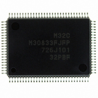
Manufacturer Part Number
M30833FJFP#U5
Description
IC M32C/83 MCU FLASH 100QFP
Manufacturer
Renesas Electronics America
Series
M16C™ M32C/80r
Datasheets
1.M3087BFLGPU3.pdf
(364 pages)
2.M30833FJGPU3.pdf
(96 pages)
3.M30833FJGPU3.pdf
(529 pages)
Specifications of M30833FJFP#U5
Core Processor
M32C/80
Core Size
16/32-Bit
Speed
32MHz
Connectivity
CAN, I²C, IEBus, SIO, UART/USART
Peripherals
DMA, WDT
Number Of I /o
85
Program Memory Size
512KB (512K x 8)
Program Memory Type
FLASH
Ram Size
31K x 8
Voltage - Supply (vcc/vdd)
3 V ~ 5.5 V
Data Converters
A/D 26x10b; D/A 2x8b
Oscillator Type
Internal
Operating Temperature
-20°C ~ 85°C
Package / Case
100-QFP
For Use With
R0K330879S001BE - KIT DEV RSK M32C/87R0K330879S000BE - KIT DEV RSK M32C/87
Lead Free Status / RoHS Status
Lead free / RoHS Compliant
Eeprom Size
-
Available stocks
Company
Part Number
Manufacturer
Quantity
Price

Part Number:
M30833FJFP#U5M30833FJFP#U3
Manufacturer:
Renesas Electronics America
Quantity:
135
Part Number:
M30833FJFP#U5M30833FJFP#U3
Manufacturer:
Renesas Electronics America
Quantity:
10 000


R
R
M
1.6 Pin Description
e
E
3
. v
J
2
I : Input
NOTES:
0
Table 1.6 Pin Description (100-Pin and 144-Pin Packages)
Power Supply
Analog Power
Supply
Reset Input
CNV
Input to Switch
External Data Bus
Width
Bus Control
Pins
DRAM Bus
Control Pin
Classsfication
C
1
9
3 .
B
1. Apply 4.2 to 5.5V to the V
2. Bus control pins in M32C/83T cannot be used.
8 /
0
1
3
(2)
SS
0
(2)
3
J
G
4
a
o r
0 -
n
O : Output
3 .
(2)
u
1
, 1
3
p
1
(
2
M
0
______
_________
__________
________
__________
________
0
3
V
V
AV
AV
____________
RESET
CNV
BYTE
D
D
A
A
A
A
A
A
CS0 to CS3
________
WRL / WR
WRH / BHE
_____
RD
ALE
__________
HOLD
HLDA
RDY
MA
______
DW
CASL
__________
CASH
RAS
______
6
2
Symbol
CC
SS
0
23
0
7
8
15
0
8
/D
/D
/D
C
0
CC
SS
to D
to D
to A
/D
to MA
8 /
SS
0
7
8
15
Page 14
, 3
to
to
I/O : Input and output
________
______
22
7
15
______
12
M
CC
3
I/O Type
2
pin when using M32C/83T.
C
I/O
I/O
I/O
I/O
f o
O
O
O
O
O
O
O
O
8 /
I
I
I
I
I
I
I
4
3
8
) T
8
Apply 3.0 to 5.5V to both V
Apply 0V to the V
Supplies power to the A/D converter. Connect the AV
AV
The microcomputer is in a reset state when "L" is applied to the RESET pin
Switches processor mode. Connect the CNV
chip mode or to V
Switches data bus width in external memory space 3. The data bus is 16
bits wide when the BYTE pin is held "L" and 8 bits wide when it is held "H".
Set to either. Connect the BYTE pin to V
single-chip mode
Inputs and outputs data (D
space with separate bus
Inputs and outputs data (D
space with 16-bit separate bus
Outputs address bits A
Outputs inversed address bit A
Inputs and outputs data (D
to A
multiplexed bus
Inputs and outputs data (D
(A
16-bit multiplexed bus
Outputs CS0 to CS3 that are chip-select signals specifying an external space
Outputs WRL, WRH, (WR, BHE) and RD signals. WRL and WRH can be
switched with WR and BHE by program
ALE is a signal latching the address
The microcomputer is placed in a hold state while the HOLD pin is held "L"
Outputs an "L" signal while the microcomputer is placed in a hold state
Bus is placed in a wait state while the RDY pin is held "L"
When DRAM area is accessed, outputs column and row addresses by time-sharing.
The DW signal becomes "L" when data is written to the DRAM area. CASL and CASH are
signals indicating the timing to latch column addresses. The CASL signal becomes "L" when
an even address is accessed. The CASH signal becomes "L" when an odd address is
accessed. RAS is a signal latching row addresses.
________
WRL, WRH and RD selected:
______ ________
WR, BHE and RD selected:
8
SS
If external data bus is 16 bits wide, data is written to an even address in
external memory space when WRL is held "L".
Data is written to an odd address when WRH is held "L".
Data is read when RD is held "L".
Data is written to external memory space when WR is held "L".
Data in an external memory space is read when RD is held "L".
An odd address is accessed when BHE is held "L".
Select WR, BHE and RD for external 8-bit data bus.
______
to A
7
) by time-sharing while accessing an external memory space with
pin to V
_______
15
_________
________
________
) by time-sharing while accessing an external memory space with
______ ________
_______
SS
______
_________
CC
_____
SS
_____
to start up in microprocessor mode
pin.
_____
______ ________
0
_______
to A
_____
(1)
0
8
0
8
CC
to D
to D
to D
to D
__________
22
Function
pin.
23
7
15
7
15
________
) while accessing an external memory
) and outputs 8 low-order address bits (A
) while accessing an external memory
) and outputs 8 middle-order address bits
_____
________
________
SS
_________
SS
to use the microcomputer in
pin to V
__________
__________
______
________
_____
SS
CC
__________
___________
to start up in single-
pin to V
_________
CC
__________
1. Overview
and the
0
Related parts for M30833FJFP#U5
Image
Part Number
Description
Manufacturer
Datasheet
Request
R

Part Number:
Description:
KIT STARTER FOR M16C/29
Manufacturer:
Renesas Electronics America
Datasheet:

Part Number:
Description:
KIT STARTER FOR R8C/2D
Manufacturer:
Renesas Electronics America
Datasheet:

Part Number:
Description:
R0K33062P STARTER KIT
Manufacturer:
Renesas Electronics America
Datasheet:

Part Number:
Description:
KIT STARTER FOR R8C/23 E8A
Manufacturer:
Renesas Electronics America
Datasheet:

Part Number:
Description:
KIT STARTER FOR R8C/25
Manufacturer:
Renesas Electronics America
Datasheet:

Part Number:
Description:
KIT STARTER H8S2456 SHARPE DSPLY
Manufacturer:
Renesas Electronics America
Datasheet:

Part Number:
Description:
KIT STARTER FOR R8C38C
Manufacturer:
Renesas Electronics America
Datasheet:

Part Number:
Description:
KIT STARTER FOR R8C35C
Manufacturer:
Renesas Electronics America
Datasheet:

Part Number:
Description:
KIT STARTER FOR R8CL3AC+LCD APPS
Manufacturer:
Renesas Electronics America
Datasheet:
Part Number:
Description:
KIT STARTER FOR RX610
Manufacturer:
Renesas Electronics America
Datasheet:

Part Number:
Description:
KIT STARTER FOR R32C/118
Manufacturer:
Renesas Electronics America
Datasheet:

Part Number:
Description:
KIT DEV RSK-R8C/26-29
Manufacturer:
Renesas Electronics America
Datasheet:

Part Number:
Description:
KIT STARTER FOR SH7124
Manufacturer:
Renesas Electronics America
Datasheet:

Part Number:
Description:
KIT STARTER FOR H8SX/1622
Manufacturer:
Renesas Electronics America
Datasheet:

Part Number:
Description:
KIT DEV FOR SH7203
Manufacturer:
Renesas Electronics America
Datasheet: