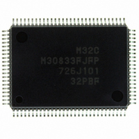
M30833FJFP#U5 Renesas Electronics America, M30833FJFP#U5 Datasheet - Page 488

M30833FJFP#U5
Manufacturer Part Number
M30833FJFP#U5
Description
IC M32C/83 MCU FLASH 100QFP
Manufacturer
Renesas Electronics America
Series
M16C™ M32C/80r
Datasheets
1.M3087BFLGPU3.pdf
(364 pages)
2.M30833FJGPU3.pdf
(96 pages)
3.M30833FJGPU3.pdf
(529 pages)
Specifications of M30833FJFP#U5
Core Processor
M32C/80
Core Size
16/32-Bit
Speed
32MHz
Connectivity
CAN, I²C, IEBus, SIO, UART/USART
Peripherals
DMA, WDT
Number Of I /o
85
Program Memory Size
512KB (512K x 8)
Program Memory Type
FLASH
Ram Size
31K x 8
Voltage - Supply (vcc/vdd)
3 V ~ 5.5 V
Data Converters
A/D 26x10b; D/A 2x8b
Oscillator Type
Internal
Operating Temperature
-20°C ~ 85°C
Package / Case
100-QFP
For Use With
R0K330879S001BE - KIT DEV RSK M32C/87R0K330879S000BE - KIT DEV RSK M32C/87
Lead Free Status / RoHS Status
Lead free / RoHS Compliant
Eeprom Size
-
Available stocks
Company
Part Number
Manufacturer
Quantity
Price
Part Number:
M30833FJFP#U5M30833FJFP#U3
Manufacturer:
Renesas Electronics America
Quantity:
135
Part Number:
M30833FJFP#U5M30833FJFP#U3
Manufacturer:
Renesas Electronics America
Quantity:
10 000
- Current page: 488 of 529
- Download datasheet (5Mb)
R
R
M
27.2 Bus
e
E
3
. v
J
2
0
27.2.1 HOLD Signal
27.2.2 External Bus
C
1
9
3 .
B
8 /
When entering microprocessor mode or memory expansion mode from single-chip mode and using
__________
HOLD input, set the PM01 to PM00 bits to "11
mode) after setting the PD4_0 to PD4_7 bits in the PD4 register and the PD5_0 to PD5_2 bits in the PD5
register to "0" (input mode).
P4
not enter a high-impedance state even when an "L" signal is applied to the HOLD pin, if the PM01 to
PM00 bits are set to "11
PD4_0 to PD4_7 bits in the PD4 register and the PD5_0 to PD5_2 bits in the PD5 register to "1" (output
mode) in single-chip mode.
The internal ROM cannot be read when an "H" signal is applied to the CNV
(hardware reset 1 or hardware reset 2) occurs.
0
1
3
0
0
3
J
G
to P4
4
a
o r
0 -
n
3 .
__________
1
u
, 1
3
p
7
1
(
2
(A
M
0
0
16
3
6
2
to A
C
Page 463
8 /
, 3
22
, A
M
_____
3
2
23
" (microprocessor mode) or to "10
2
C
, CS0 to CS3, MA8 to MA12) and P5
f o
_______
8 /
4
3
8
) T
8
_______
2
" (microprocessor mode) or to "10
2
" (memory expansion mode) after setting the
0
to P5
2
(RD/WR/BHE, RD/WRL,WRH) do
______ ______ ________ ______ _______ ________
SS
pin and the hardware reset
__________
2
" (memory expansion
27. Precautions (Bus)
Related parts for M30833FJFP#U5
Image
Part Number
Description
Manufacturer
Datasheet
Request
R

Part Number:
Description:
KIT STARTER FOR M16C/29
Manufacturer:
Renesas Electronics America
Datasheet:

Part Number:
Description:
KIT STARTER FOR R8C/2D
Manufacturer:
Renesas Electronics America
Datasheet:

Part Number:
Description:
R0K33062P STARTER KIT
Manufacturer:
Renesas Electronics America
Datasheet:

Part Number:
Description:
KIT STARTER FOR R8C/23 E8A
Manufacturer:
Renesas Electronics America
Datasheet:

Part Number:
Description:
KIT STARTER FOR R8C/25
Manufacturer:
Renesas Electronics America
Datasheet:

Part Number:
Description:
KIT STARTER H8S2456 SHARPE DSPLY
Manufacturer:
Renesas Electronics America
Datasheet:

Part Number:
Description:
KIT STARTER FOR R8C38C
Manufacturer:
Renesas Electronics America
Datasheet:

Part Number:
Description:
KIT STARTER FOR R8C35C
Manufacturer:
Renesas Electronics America
Datasheet:

Part Number:
Description:
KIT STARTER FOR R8CL3AC+LCD APPS
Manufacturer:
Renesas Electronics America
Datasheet:

Part Number:
Description:
KIT STARTER FOR RX610
Manufacturer:
Renesas Electronics America
Datasheet:

Part Number:
Description:
KIT STARTER FOR R32C/118
Manufacturer:
Renesas Electronics America
Datasheet:

Part Number:
Description:
KIT DEV RSK-R8C/26-29
Manufacturer:
Renesas Electronics America
Datasheet:

Part Number:
Description:
KIT STARTER FOR SH7124
Manufacturer:
Renesas Electronics America
Datasheet:

Part Number:
Description:
KIT STARTER FOR H8SX/1622
Manufacturer:
Renesas Electronics America
Datasheet:

Part Number:
Description:
KIT DEV FOR SH7203
Manufacturer:
Renesas Electronics America
Datasheet:


