M30833FJFP#U5 Renesas Electronics America, M30833FJFP#U5 Datasheet - Page 148
M30833FJFP#U5
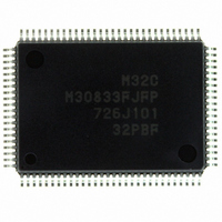
Manufacturer Part Number
M30833FJFP#U5
Description
IC M32C/83 MCU FLASH 100QFP
Manufacturer
Renesas Electronics America
Series
M16C™ M32C/80r
Datasheets
1.M3087BFLGPU3.pdf
(364 pages)
2.M30833FJGPU3.pdf
(96 pages)
3.M30833FJGPU3.pdf
(529 pages)
Specifications of M30833FJFP#U5
Core Processor
M32C/80
Core Size
16/32-Bit
Speed
32MHz
Connectivity
CAN, I²C, IEBus, SIO, UART/USART
Peripherals
DMA, WDT
Number Of I /o
85
Program Memory Size
512KB (512K x 8)
Program Memory Type
FLASH
Ram Size
31K x 8
Voltage - Supply (vcc/vdd)
3 V ~ 5.5 V
Data Converters
A/D 26x10b; D/A 2x8b
Oscillator Type
Internal
Operating Temperature
-20°C ~ 85°C
Package / Case
100-QFP
For Use With
R0K330879S001BE - KIT DEV RSK M32C/87R0K330879S000BE - KIT DEV RSK M32C/87
Lead Free Status / RoHS Status
Lead free / RoHS Compliant
Eeprom Size
-
Available stocks
Company
Part Number
Manufacturer
Quantity
Price

Part Number:
M30833FJFP#U5M30833FJFP#U3
Manufacturer:
Renesas Electronics America
Quantity:
135
Part Number:
M30833FJFP#U5M30833FJFP#U3
Manufacturer:
Renesas Electronics America
Quantity:
10 000


R
R
M
e
E
12.2 DMAC Transfer Cycles
12.3 Channel Priority and DMA Transfer Timing
3
. v
J
i= 0 to 3, p = 0 to 1
Table 12.3 DMAC Transfer Cycles
Table 12.4 Coefficient j, k
2
0
n I
n I
k
w
= j
The number of DMAC transfer cycle can be calculated as follows.
Any combination of even or odd transfer read and write addresses are possible. Table 12.3 lists the number
of DMAC transfer cycles. Table 12.4 lists coefficient j, k.
Transfer Unit
8-bit transfers
(BWi bit in the DMDp
16-bit transfers
(BWi bit = 1)
When multiple DMA requests are generated in the same sampling period, between the falling edge of the
CPU clock and the next falling edge, the DRQ bit in the DMiSL register (i = 0 to 3) is set to "1" (requested)
simultaneously. Channel priority in this case is : DMA0 > DMA1 > DMA2 > DMA3.
Figure 12.7 shows an example of the DMA transfer by external factors.
In Figure 12.7, the DMA0 request having the highest priority is received first to start a transfer when a DMA0
request and DMA1 request are generated simultaneously. After one DMA0 transfer is completed, the bus
privilege is returned to the CPU. When the CPU has completed one bus access, the DMA1 transfer starts.
After one DMA1 transfer is completed, the privilege is again returned to the CPU.
In addition, DMA requests cannot be counted up since each channel has one DRQ bit. Therefore, when
DMA requests, as DMA1 in Figure 12.7, occur more than once before receiving bus privilege, the DRQ bit
is set to "0" as soon as privilege is acquired. The bus privilege is returned to the CPU when one transfer is
completed.
1
C
9
register = 0)
e t
e t
h t i
=
3 .
B
8 /
Transfer cycles per transfer = Number of read cycle x j + Number of write cycle x k
1
n r
n r
1
0
1
n
3
0
l a
l a
o
3
J
G
R
R
w
4
a
0 -
n
o r
O
A
i a
3 .
M
s t
M
1
u
, 1
3
p
a t
r o
1
e t
2
(
n I
M
0
e t
0
3
n I
n I
a
k
= j
6
n r
2
e t
e t
=
w
l a
C
2
n r
n r
i a
2
8 /
Page 123
S
s t
l a
l a
p
, 3
a
a t
Bus Width Access Address
R
R
e c
e t
O
A
16-bit
16-bit
M
8-bit
8-bit
M
M
3
w
2
r o
C
h t i
f o
8 /
4
3
8
k
S
A
= j
) T
8
F
e r
=
R
2
a
2
B
S
w
k
= j
Even
Even
Even
Even
Odd
Odd
Odd
Odd
s u
e
i a
=
p
1
s t
2
a
w
a r
a t
h t i
e t
e t
n
o
B
k
S
w
j
s u
=
e
i a
=
p
s t
2
Cycle
a
2
Read
w
a r
a t
Single-Chip Mode
—
—
—
—
h t i
1
1
1
2
e t
e t
1
S
B
k
w
j
e
s u
=
i a
=
p
s t
3
a
3
w
E
a r
t a t
h t i
x
e t
r e t
Cycle
Write
s e
2
a n
—
—
—
—
1
1
1
2
S l
S
B
k
w
j
a p
s u
e
=
i a
=
p
s t
e c
4
a
4
w
a r
t a t
h t i
e t
Memory Expansion Mode
s e
3
Microprocessor Mode
Cycle
Read
M
B
k
w
j
1
1
1
1
1
2
2
2
s u
=
i a
l u
=
s t
p i t
3
3
w
e l
t a t
h t i
e x
s e
2
d
Cycle
Write
M
B
k
w
j
s u
=
l u
i a
=
1
1
1
1
1
2
2
2
s t
p i t
12. DMAC
4
4
w
e l
t a t
h t i
e x
s e
3
d
Related parts for M30833FJFP#U5
Image
Part Number
Description
Manufacturer
Datasheet
Request
R

Part Number:
Description:
KIT STARTER FOR M16C/29
Manufacturer:
Renesas Electronics America
Datasheet:

Part Number:
Description:
KIT STARTER FOR R8C/2D
Manufacturer:
Renesas Electronics America
Datasheet:

Part Number:
Description:
R0K33062P STARTER KIT
Manufacturer:
Renesas Electronics America
Datasheet:

Part Number:
Description:
KIT STARTER FOR R8C/23 E8A
Manufacturer:
Renesas Electronics America
Datasheet:

Part Number:
Description:
KIT STARTER FOR R8C/25
Manufacturer:
Renesas Electronics America
Datasheet:

Part Number:
Description:
KIT STARTER H8S2456 SHARPE DSPLY
Manufacturer:
Renesas Electronics America
Datasheet:

Part Number:
Description:
KIT STARTER FOR R8C38C
Manufacturer:
Renesas Electronics America
Datasheet:

Part Number:
Description:
KIT STARTER FOR R8C35C
Manufacturer:
Renesas Electronics America
Datasheet:

Part Number:
Description:
KIT STARTER FOR R8CL3AC+LCD APPS
Manufacturer:
Renesas Electronics America
Datasheet:
Part Number:
Description:
KIT STARTER FOR RX610
Manufacturer:
Renesas Electronics America
Datasheet:

Part Number:
Description:
KIT STARTER FOR R32C/118
Manufacturer:
Renesas Electronics America
Datasheet:

Part Number:
Description:
KIT DEV RSK-R8C/26-29
Manufacturer:
Renesas Electronics America
Datasheet:

Part Number:
Description:
KIT STARTER FOR SH7124
Manufacturer:
Renesas Electronics America
Datasheet:

Part Number:
Description:
KIT STARTER FOR H8SX/1622
Manufacturer:
Renesas Electronics America
Datasheet:

Part Number:
Description:
KIT DEV FOR SH7203
Manufacturer:
Renesas Electronics America
Datasheet: