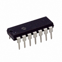
PIC16F526-I/P Microchip Technology, PIC16F526-I/P Datasheet - Page 56

PIC16F526-I/P
Manufacturer Part Number
PIC16F526-I/P
Description
IC PIC MCU FLASH 1KX12 14DIP
Manufacturer
Microchip Technology
Series
PIC® 16Fr
Datasheets
1.PIC16F526-ISL.pdf
(122 pages)
2.PIC16F526-ISL.pdf
(22 pages)
3.PIC16F526-IP.pdf
(104 pages)
Specifications of PIC16F526-I/P
Program Memory Type
FLASH
Program Memory Size
1.5KB (1K x 12)
Package / Case
14-DIP (0.300", 7.62mm)
Core Processor
PIC
Core Size
8-Bit
Speed
20MHz
Peripherals
POR, WDT
Number Of I /o
11
Ram Size
67 x 8
Voltage - Supply (vcc/vdd)
2 V ~ 5.5 V
Data Converters
A/D 3x8b
Oscillator Type
Internal
Operating Temperature
-40°C ~ 85°C
Processor Series
PIC16F
Core
PIC
Data Bus Width
8 bit
Data Ram Size
67 B
Maximum Clock Frequency
20 MHz
Number Of Programmable I/os
12
Number Of Timers
1
Maximum Operating Temperature
+ 85 C
Mounting Style
Through Hole
3rd Party Development Tools
52715-96, 52716-328, 52717-734
Development Tools By Supplier
PG164130, DV164035, DV244005, DV164005, PG164120, ICE2000
Minimum Operating Temperature
- 40 C
On-chip Adc
8 bit, 3 Channel
Lead Free Status / RoHS Status
Lead free / RoHS Compliant
For Use With
AC162096 - HEADER MPLAB ICD2 PIC16F526 8/14
Eeprom Size
-
Connectivity
-
Lead Free Status / Rohs Status
Lead free / RoHS Compliant
PIC16F526
8.9
A device may be powered down (Sleep) and later
powered up (wake-up from Sleep).
8.9.1
The Power-Down mode is entered by executing a
SLEEP instruction.
If enabled, the Watchdog Timer will be cleared but
keeps running, the TO bit of the STATUS register is set,
the PD bit of the STATUS register is cleared and the
oscillator driver is turned off. The I/O ports maintain the
status they had before the SLEEP instruction was exe-
cuted (driving high, driving low or high-impedance).
For lowest current consumption while powered down,
the T0CKI input should be at V
MCLR/V
enabled.
DS41326E-page 56
Note:
PP
Power-down Mode (Sleep)
pin must be at a logic high level if MCLR is
SLEEP
A Reset generated by a WDT time-out
does not drive the MCLR pin low.
DD
or V
SS
and the RB3/
8.9.2
The device can wake-up from Sleep through one of
the following events:
1.
2.
3.
4.
These events cause a device Reset. The TO, PD and
CWUF/RBWUF bits can be used to determine the
cause of device Reset. The TO bit is cleared if a WDT
time-out occurred (and caused wake-up). The PD bit,
which is set on power-up, is cleared when SLEEP is
invoked. The CWUF bit indicates a change in a com-
parator output state while the device was in Sleep. The
RBWUF bit indicates a change in state while in Sleep
at pins RB0, RB1, RB3 or RB4 (since the last file or bit
operation on RB port).
The WDT is cleared when the device wakes from
Sleep, regardless of the wake-up source.
Note:
Note:
An external Reset input on RB3/MCLR/V
when configured as MCLR.
A Watchdog Timer Time-out Reset (if WDT was
enabled).
A change on input pin RB0, RB1, RB3 or RB4
when wake-up on change is enabled.
A change in one of the comparator output bits,
C1OUT or C2OUT (if comparator wake-up is
enabled).
WAKE-UP FROM SLEEP
Caution: Right before entering Sleep,
read the input pins. When in Sleep,
wake-up occurs when the values at the
pins change from the state they were in at
the last reading. If a wake-up on change
occurs and the pins are not read before
re-entering Sleep, a wake-up will occur
immediately even if no pins change while
in Sleep mode.
Caution: Right before entering Sleep,
read
register(s) CM1CON0 and CM2CON0.
When in Sleep, wake-up occurs when the
comparator output bit C1OUT and C2OUT
change from the state they were in at the
last reading. If a wake-up on comparator
change occurs and the pins are not read
before re-entering Sleep, a wake-up will
occur immediately, even if no pins change
while in Sleep mode.
the
2010 Microchip Technology Inc.
comparator
Configuration
PP
pin,


