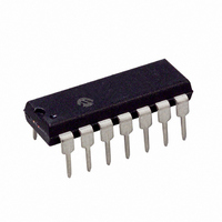
PIC16F526-I/P Microchip Technology, PIC16F526-I/P Datasheet - Page 22

PIC16F526-I/P
Manufacturer Part Number
PIC16F526-I/P
Description
IC PIC MCU FLASH 1KX12 14DIP
Manufacturer
Microchip Technology
Series
PIC® 16Fr
Datasheets
1.PIC16F526-ISL.pdf
(122 pages)
2.PIC16F526-ISL.pdf
(22 pages)
3.PIC16F526-IP.pdf
(104 pages)
Specifications of PIC16F526-I/P
Program Memory Type
FLASH
Program Memory Size
1.5KB (1K x 12)
Package / Case
14-DIP (0.300", 7.62mm)
Core Processor
PIC
Core Size
8-Bit
Speed
20MHz
Peripherals
POR, WDT
Number Of I /o
11
Ram Size
67 x 8
Voltage - Supply (vcc/vdd)
2 V ~ 5.5 V
Data Converters
A/D 3x8b
Oscillator Type
Internal
Operating Temperature
-40°C ~ 85°C
Processor Series
PIC16F
Core
PIC
Data Bus Width
8 bit
Data Ram Size
67 B
Maximum Clock Frequency
20 MHz
Number Of Programmable I/os
12
Number Of Timers
1
Maximum Operating Temperature
+ 85 C
Mounting Style
Through Hole
3rd Party Development Tools
52715-96, 52716-328, 52717-734
Development Tools By Supplier
PG164130, DV164035, DV244005, DV164005, PG164120, ICE2000
Minimum Operating Temperature
- 40 C
On-chip Adc
8 bit, 3 Channel
Lead Free Status / RoHS Status
Lead free / RoHS Compliant
For Use With
AC162096 - HEADER MPLAB ICD2 PIC16F526 8/14
Eeprom Size
-
Connectivity
-
Lead Free Status / Rohs Status
Lead free / RoHS Compliant
PIC16F526
4.8
The INDF Register is not a physical register.
Addressing INDF actually addresses the register
whose address is contained in the FSR Register (FSR
is a pointer). This is indirect addressing.
Reading INDF itself indirectly (FSR = 0) will produce
00h. Writing to the INDF Register indirectly results in a
no-operation (although Status bits may be affected).
The FSR is an 8-bit wide register. It is used in
conjunction with the INDF Register to indirectly
address the data memory area.
The FSR<4:0> bits are used to select data memory
addresses 00h to 1Fh.
FSR<6:5> are the bank select bits and are used to
select the bank to be addressed (00 = Bank 0,
01 = Bank 1, 10 = Bank 2, 11 = Bank 3).
FSR<7> is unimplemented and read as ‘1’.
FIGURE 4-4:
DS41326E-page 22
bank select
Note 1: For register map detail see Figure 4-1.
(FSR)
6
Indirect Data Addressing: INDF
and FSR Registers
5
Direct Addressing
location select
Data
Memory
4
DIRECT/INDIRECT ADDRESSING
3
(opcode)
(1)
2
00h
0Ch
0Dh
0Fh
10h
1Fh
1
0
Bank 0
00
2Fh
3Fh
Bank 1
01
Addresses map back to
addresses in Bank 0.
4Fh
5Fh
Bank 2
10
A simple program to clear RAM locations 10h-1Fh
using indirect addressing is shown in Example 4-1.
EXAMPLE 4-1:
NEXT
CONTINUE
6Fh
7Fh
Bank 3
11
MOVLW
MOVWF
CLRF
INCF
BTFSC
GOTO
:
:
0x10
FSR
INDF
FSR,F
FSR,4
NEXT
HOW TO CLEAR RAM
USING INDIRECT
ADDRESSING
2010 Microchip Technology Inc.
6
;initialize pointer
;to RAM
;clear INDF
;register
;inc pointer
;all done?
;NO, clear next
;YES, continue
Indirect Addressing
bank
select
5
4
(FSR)
3
location select
2
1
0


