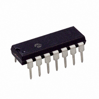
PIC16F526-I/P Microchip Technology, PIC16F526-I/P Datasheet - Page 13

PIC16F526-I/P
Manufacturer Part Number
PIC16F526-I/P
Description
IC PIC MCU FLASH 1KX12 14DIP
Manufacturer
Microchip Technology
Series
PIC® 16Fr
Datasheets
1.PIC16F526-ISL.pdf
(122 pages)
2.PIC16F526-ISL.pdf
(22 pages)
3.PIC16F526-IP.pdf
(104 pages)
Specifications of PIC16F526-I/P
Program Memory Type
FLASH
Program Memory Size
1.5KB (1K x 12)
Package / Case
14-DIP (0.300", 7.62mm)
Core Processor
PIC
Core Size
8-Bit
Speed
20MHz
Peripherals
POR, WDT
Number Of I /o
11
Ram Size
67 x 8
Voltage - Supply (vcc/vdd)
2 V ~ 5.5 V
Data Converters
A/D 3x8b
Oscillator Type
Internal
Operating Temperature
-40°C ~ 85°C
Processor Series
PIC16F
Core
PIC
Data Bus Width
8 bit
Data Ram Size
67 B
Maximum Clock Frequency
20 MHz
Number Of Programmable I/os
12
Number Of Timers
1
Maximum Operating Temperature
+ 85 C
Mounting Style
Through Hole
3rd Party Development Tools
52715-96, 52716-328, 52717-734
Development Tools By Supplier
PG164130, DV164035, DV244005, DV164005, PG164120, ICE2000
Minimum Operating Temperature
- 40 C
On-chip Adc
8 bit, 3 Channel
Lead Free Status / RoHS Status
Lead free / RoHS Compliant
For Use With
AC162096 - HEADER MPLAB ICD2 PIC16F526 8/14
Eeprom Size
-
Connectivity
-
Lead Free Status / Rohs Status
Lead free / RoHS Compliant
TABLE 3-2:
2010 Microchip Technology Inc.
RB0//C1IN+/AN0/
ICSPDAT
RB1/C1IN-/AN1/
ICSPCLK
RB2/C1OUT/AN2
RB3/MCLR/V
RB4/OSC2/CLKOUT
RB5/OSC1/CLKIN
RC0/C2IN+
RC1/C2IN-
RC2/CV
RC3
RC4/C2OUT
RC5/T0CKI
V
V
Legend: I = Input, O = Output, I/O = Input/Output, P = Power, — = Not used, TTL = TTL input,
DD
SS
REF
Name
ST = Schmitt Trigger input, HV = High Voltage
PP
PIC16F526 PINOUT DESCRIPTION
Function
ICSPDAT
ICSPCLK
CLKOUT
C1OUT
C2OUT
C1IN+
CLKIN
C2IN+
CV
MCLR
OSC2
OSC1
T0CKI
C1IN-
C2IN-
RB0
AN0
RB1
AN1
RB2
AN2
RB3
RB4
RB5
RC0
RC1
RC2
RC3
RC4
RC5
V
V
V
DD
PP
SS
REF
Input
XTAL
Type
TTL
TTL
TTL
TTL
TTL
TTL
TTL
TTL
TTL
TTL
TTL
TTL
AN
AN
ST
AN
AN
ST
AN
ST
HV
ST
AN
AN
ST
—
—
—
—
—
—
—
Output
CMOS Bidirectional I/O pin. Can be software programmed for internal
CMOS ICSP™ mode Schmitt Trigger.
CMOS Bidirectional I/O pin. Can be software programmed for internal
CMOS ICSP mode Schmitt Trigger.
CMOS Bidirectional I/O pin.
CMOS Comparator 1 output.
CMOS Bidirectional I/O pin. Can be software programmed for internal
CMOS EXTRC/INTRC CLKOUT pin (F
CMOS Bidirectional I/O pin.
CMOS Bidirectional I/O port.
CMOS Bidirectional I/O port.
CMOS Bidirectional I/O port.
CMOS Bidirectional I/O port.
CMOS Bidirectional I/O port.
CMOS Comparator 2 output.
CMOS Bidirectional I/O port.
XTAL
Type
AN
—
—
—
—
—
—
—
—
—
—
—
—
—
P
P
weak pull-up and wake-up from Sleep on pin change.
Comparator 1 input.
ADC channel input.
weak pull-up and wake-up from Sleep on pin change.
Comparator 1 input.
ADC channel input.
ADC channel input.
Input pin. Can be software programmed for internal weak
pull-up and wake-up from Sleep on pin change.
Master Clear (Reset). When configured as MCLR, this pin is
an active-low Reset to the device. Voltage on MCLR/V
not exceed V
will enter Programming mode. Weak pull-up always on if
configured as MCLR.
Programming voltage input.
weak pull-up and wake-up from Sleep on pin change.
Oscillator crystal output. Connections to crystal or resonator in
Crystal Oscillator mode (XT, HS and LP modes only, PORTB
in other modes).
Oscillator crystal input.
External clock source input.
Comparator 2 input.
Comparator 2 input.
Programmable Voltage Reference output.
Timer0 Schmitt Trigger input pin.
Positive supply for logic and I/O pins.
Ground reference for logic and I/O pins.
DD
during normal device operation or the device
Description
OSC
PIC16F526
/4).
DS41326E-page 13
PP
must


