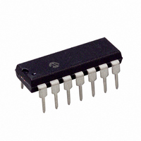
PIC16F526-I/P Microchip Technology, PIC16F526-I/P Datasheet - Page 23

PIC16F526-I/P
Manufacturer Part Number
PIC16F526-I/P
Description
IC PIC MCU FLASH 1KX12 14DIP
Manufacturer
Microchip Technology
Series
PIC® 16Fr
Datasheets
1.PIC16F526-ISL.pdf
(122 pages)
2.PIC16F526-ISL.pdf
(22 pages)
3.PIC16F526-IP.pdf
(104 pages)
Specifications of PIC16F526-I/P
Program Memory Type
FLASH
Program Memory Size
1.5KB (1K x 12)
Package / Case
14-DIP (0.300", 7.62mm)
Core Processor
PIC
Core Size
8-Bit
Speed
20MHz
Peripherals
POR, WDT
Number Of I /o
11
Ram Size
67 x 8
Voltage - Supply (vcc/vdd)
2 V ~ 5.5 V
Data Converters
A/D 3x8b
Oscillator Type
Internal
Operating Temperature
-40°C ~ 85°C
Processor Series
PIC16F
Core
PIC
Data Bus Width
8 bit
Data Ram Size
67 B
Maximum Clock Frequency
20 MHz
Number Of Programmable I/os
12
Number Of Timers
1
Maximum Operating Temperature
+ 85 C
Mounting Style
Through Hole
3rd Party Development Tools
52715-96, 52716-328, 52717-734
Development Tools By Supplier
PG164130, DV164035, DV244005, DV164005, PG164120, ICE2000
Minimum Operating Temperature
- 40 C
On-chip Adc
8 bit, 3 Channel
Lead Free Status / RoHS Status
Lead free / RoHS Compliant
For Use With
AC162096 - HEADER MPLAB ICD2 PIC16F526 8/14
Eeprom Size
-
Connectivity
-
Lead Free Status / Rohs Status
Lead free / RoHS Compliant
5.0
The Flash data memory is readable and writable during
normal operation (full V
directly mapped in the register file space. Instead, it is
indirectly addressed through the Special Function
Registers (SFRs).
5.1
To read a Flash data memory location the user must:
• Write the EEADR register
• Set the RD bit of the EECON register
The value written to the EEADR register determines
which Flash data memory location is read. Setting the
RD bit of the EECON register initiates the read. Data
from the Flash data memory read is available in the
EEDATA register immediately. The EEDATA register
will hold this value until another read is initiated or it is
modified by a write operation. Program execution is
suspended while the read cycle is in progress.
Execution will continue with the instruction following the
one that sets the WR bit. See Example 1 for sample
code.
EXAMPLE 1:
5.2
Flash data memory is erased one row at a time and
written one byte at a time. The 64-byte array is made
up of eight rows. A row contains eight sequential bytes.
Row boundaries exist every eight bytes.
Generally, the procedure to write a byte of data to Flash
data memory is:
1.
2.
2010 Microchip Technology Inc.
Note: Only a BSF command will work to enable the
BANKSEL EEADR
MOVF DATA_EE_ADDR, W
MOVWF EEADR
BANKSEL EECON1
BSF EECON, RD
MOVF EEDATA, W
Identify the row containing the address where
the byte will be written.
If there is other information in that row that must
be saved, copy those bytes from Flash data
memory to RAM.
FLASH DATA MEMORY
CONTROL
Reading Flash Data Memory
Writing and Erasing Flash Data
Memory
Flash data memory read documented in
Example 1.
commands will work, no exceptions.
READING FROM FLASH
DATA MEMORY
DD
No
range). This memory is not
;
;
;Data Memory
;Address to read
;
;EE Read
;W = EEDATA
other
sequence
of
3.
4.
To prevent accidental corruption of the Flash data
memory, an unlock sequence is required to initiate a
write or erase cycle. This sequence requires that the bit
set instructions used to configure the EECON register
happen exactly as shown in Example 2 and Example 3,
depending on the operation requested.
5.2.1
A row must be manually erased before writing new
data. The following sequence must be performed for a
single row erase.
1.
2.
3.
4.
If the WREN bit is not set in the instruction cycle after
the FREE bit is set, the FREE bit will be cleared in
hardware.
If the WR bit is not set in the instruction cycle after the
WREN bit is set, the WREN bit will be cleared in
hardware.
Sample code that follows this procedure is included in
Example 2.
Program execution is suspended while the erase cycle
is in progress. Execution will continue with the
instruction following the one that sets the WR bit.
EXAMPLE 2:
BANKSEL
MOVLW
MOVWF
BSF
BSF
BSF
Note 1: The FREE bit may be set by any com-
Perform a row erase of the row of interest.
Write the new byte of data and any saved bytes
back to the appropriate addresses in Flash data
memory.
Load EEADR with an address in the row to be
erased.
Set the FREE bit to enable the erase.
Set the WREN bit to enable write access to the
array.
Set the WR bit to initiate the erase cycle.
2: Bits <5:3> of the EEADR register indicate
ERASING FLASH DATA MEMORY
EEADR
EE_ADR_ERASE
EEADR
EECON,FREE
EECON,WREN
EECON,WR
mand normally used by the core. How-
ever, the WREN and WR bits can only be
set using a series of BSF commands, as
documented in Example 1. No other
sequence of commands will work, no
exceptions.
which row is to be erased.
ERASING A FLASH DATA
MEMORY ROW
PIC16F526
; LOAD ADDRESS OF ROW TO
; ERASE
;
; SELECT ERASE
; ENABLE WRITES
; INITITATE ERASE
DS41326E-page 23


