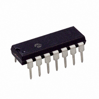
PIC16F526-I/P Microchip Technology, PIC16F526-I/P Datasheet - Page 18

PIC16F526-I/P
Manufacturer Part Number
PIC16F526-I/P
Description
IC PIC MCU FLASH 1KX12 14DIP
Manufacturer
Microchip Technology
Series
PIC® 16Fr
Datasheets
1.PIC16F526-ISL.pdf
(122 pages)
2.PIC16F526-ISL.pdf
(22 pages)
3.PIC16F526-IP.pdf
(104 pages)
Specifications of PIC16F526-I/P
Program Memory Type
FLASH
Program Memory Size
1.5KB (1K x 12)
Package / Case
14-DIP (0.300", 7.62mm)
Core Processor
PIC
Core Size
8-Bit
Speed
20MHz
Peripherals
POR, WDT
Number Of I /o
11
Ram Size
67 x 8
Voltage - Supply (vcc/vdd)
2 V ~ 5.5 V
Data Converters
A/D 3x8b
Oscillator Type
Internal
Operating Temperature
-40°C ~ 85°C
Processor Series
PIC16F
Core
PIC
Data Bus Width
8 bit
Data Ram Size
67 B
Maximum Clock Frequency
20 MHz
Number Of Programmable I/os
12
Number Of Timers
1
Maximum Operating Temperature
+ 85 C
Mounting Style
Through Hole
3rd Party Development Tools
52715-96, 52716-328, 52717-734
Development Tools By Supplier
PG164130, DV164035, DV244005, DV164005, PG164120, ICE2000
Minimum Operating Temperature
- 40 C
On-chip Adc
8 bit, 3 Channel
Lead Free Status / RoHS Status
Lead free / RoHS Compliant
For Use With
AC162096 - HEADER MPLAB ICD2 PIC16F526 8/14
Eeprom Size
-
Connectivity
-
Lead Free Status / Rohs Status
Lead free / RoHS Compliant
PIC16F526
4.3
This register contains the arithmetic status of the ALU,
the Reset status and the page preselect bit.
The STATUS register can be the destination for any
instruction, as with any other register. If the STATUS
register is the destination for an instruction that affects
the Z, DC or C bits, then the write to these three bits is
disabled. These bits are set or cleared according to the
device logic. Furthermore, the TO and PD bits are not
writable. Therefore, the result of an instruction with the
STATUS register as destination may be different than
intended.
REGISTER 4-1:
DS41326E-page 18
bit 7
Legend:
R = Readable bit
-n = Value at POR
bit 7
bit 6
bit 5
bit 4
bit 3
bit 2
bit 1
bit 0
RBWUF
R/W-0
STATUS Register
RBWUF: Wake-up from Sleep on Pin Change bit
1 = Reset due to wake-up from Sleep on pin change
0 = After power-up or other Reset
CWUF: Wake-up from Sleep on Comparator Change bit
1 = Reset due to wake-up from Sleep on comparator change
0 = After power-up or other Reset
PA0: Program Page Preselect bit
1 = Page 1 (000h-1FFh)
0 = Page 0 (200h-3FFh)
TO: Time-out bit
1 = After power-up, CLRWDT instruction, or SLEEP instruction
0 = A WDT time-out occurred
PD: Power-down bit
1 = After power-up or by the CLRWDT instruction
0 = By execution of the SLEEP instruction
Z: Zero bit
1 = The result of an arithmetic or logic operation is zero
0 = The result of an arithmetic or logic operation is not zero
DC: Digit carry/borrow bit (for ADDWF and SUBWF instructions)
ADDWF:
1 = A carry from the 4th low-order bit of the result occurred
0 = A carry from the 4th low-order bit of the result did not occur
SUBWF:
1 = A borrow from the 4th low-order bit of the result did not occur
0 = A borrow from the 4th low-order bit of the result occurred
C: Carry/borrow bit (for ADDWF, SUBWF and RRF, RLF instructions)
ADDWF:
1 = A carry occurred
0 = A carry did not occur
CWUF
R/W-0
STATUS: STATUS REGISTER
W = Writable bit
‘1’ = Bit is set
R/W-0
PA0
SUBWF:
1 = A borrow did not occur
0 = A borrow occurred
R-1
TO
U = Unimplemented bit, read as ‘0’
‘0’ = Bit is cleared
For example, CLRF STATUS, will clear the upper three
bits and set the Z bit. This leaves the STATUS register
as 000u u1uu (where u = unchanged).
Therefore, it is recommended that only BCF, BSF and
MOVWF instructions be used to alter the STATUS
register. These instructions do not affect the Z, DC or C
bits from the STATUS register. For other instructions
which do affect Status bits, see Section 12.0
“Instruction Set Summary”.
R-1
PD
RRF or RLF:
Load bit with LSb or MSb, respectively
R/W-x
Z
2010 Microchip Technology Inc.
x = Bit is unknown
R/W-x
DC
R/W-x
C
bit 0


