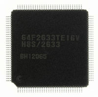
R5F61668RN50FPV Renesas Electronics America, R5F61668RN50FPV Datasheet - Page 536

R5F61668RN50FPV
Manufacturer Part Number
R5F61668RN50FPV
Description
IC H8SX/1668 MCU FLASH 144LQFP
Manufacturer
Renesas Electronics America
Series
H8® H8SX/1600r
Datasheet
1.R5F61668RN50FPV.pdf
(1506 pages)
Specifications of R5F61668RN50FPV
Core Processor
H8SX
Core Size
16/32-Bit
Speed
50MHz
Connectivity
EBI/EMI, I²C, IrDA, SCI, SmartCard, USB
Peripherals
DMA, LVD, POR, PWM, WDT
Number Of I /o
92
Program Memory Size
1MB (1M x 8)
Program Memory Type
FLASH
Ram Size
56K x 8
Voltage - Supply (vcc/vdd)
3 V ~ 3.6 V
Data Converters
A/D 8x10b; D/A 2x8b
Oscillator Type
External
Operating Temperature
-20°C ~ 75°C
Package / Case
144-LQFP
For Use With
R0K561668S000BE - KIT STARTER FOR H8SX/1668R0K561664S001BE - KIT STARTER FOR H8SX/1651HS0005KCU11H - EMULATOR E10A-USB H8S(X),SH2(A)
Lead Free Status / RoHS Status
Lead free / RoHS Compliant
Eeprom Size
-
Available stocks
Company
Part Number
Manufacturer
Quantity
Price
Company:
Part Number:
R5F61668RN50FPV
Manufacturer:
Renesas Electronics America
Quantity:
10 000
- Current page: 536 of 1506
- Download datasheet (9Mb)
Section 11 EXDMA Controller (EXDMAC)
(5)
The DTE bit in EDMDR is written to by the CPU to control enabling and disabling of data
transfer, but may be cleared to 0 automatically by the EXDMAC due to the EXDMA transfer
status.
Conditions for DTE bit clearing by the EXDMAC include the following:
• When the specified total transfer size is completely transferred
• A transfer size error interrupt is requested, and transfer ends
• A repeat size end interrupt is requested, and transfer ends
• When an extended repeat area overflow interrupt is requested, and transfer ends
• When an NMI interrupt is generated, and transfer halts
• When an address error is generated, and transfer halts
• A reset
• Hardware standby mode
• When 0 is written to the DTE bit, and transfer halts
Writes (except to the DTE bit) are prohibited to registers of a channel for which the DTE bit is set
to 1. When changing register settings after a 0-write to the DTE bit, it is necessary to confirm that
the DTE bit has been cleared to 0.
Figure 11.21 shows the procedure for changing register settings in an operating channel.
Rev. 2.00 Sep. 24, 2008 Page 502 of 1468
REJ09B0412-0200
DTE Bit in EDMDR
Figure 11.21 Procedure for Changing Register Settings in Operating Channel
Changing register settings
Change register settings
in operating channel
changes completed
Write 0 to DTE bit
Register setting
Read DTE bit
DTE bit = 0
Yes
No
[1]
[2]
[4]
[3]
[1] Write 0 to the DTE bit in EDMDR
[2] Read DTE bit.
[3] Confirm that DTE bit = 0. If DTE bit = 1,
[4] Write the required set values to the registers.
this indicates that EXDMA transfer is in progress.
Related parts for R5F61668RN50FPV
Image
Part Number
Description
Manufacturer
Datasheet
Request
R

Part Number:
Description:
KIT STARTER FOR M16C/29
Manufacturer:
Renesas Electronics America
Datasheet:

Part Number:
Description:
KIT STARTER FOR R8C/2D
Manufacturer:
Renesas Electronics America
Datasheet:

Part Number:
Description:
R0K33062P STARTER KIT
Manufacturer:
Renesas Electronics America
Datasheet:

Part Number:
Description:
KIT STARTER FOR R8C/23 E8A
Manufacturer:
Renesas Electronics America
Datasheet:

Part Number:
Description:
KIT STARTER FOR R8C/25
Manufacturer:
Renesas Electronics America
Datasheet:

Part Number:
Description:
KIT STARTER H8S2456 SHARPE DSPLY
Manufacturer:
Renesas Electronics America
Datasheet:

Part Number:
Description:
KIT STARTER FOR R8C38C
Manufacturer:
Renesas Electronics America
Datasheet:

Part Number:
Description:
KIT STARTER FOR R8C35C
Manufacturer:
Renesas Electronics America
Datasheet:

Part Number:
Description:
KIT STARTER FOR R8CL3AC+LCD APPS
Manufacturer:
Renesas Electronics America
Datasheet:

Part Number:
Description:
KIT STARTER FOR RX610
Manufacturer:
Renesas Electronics America
Datasheet:

Part Number:
Description:
KIT STARTER FOR R32C/118
Manufacturer:
Renesas Electronics America
Datasheet:

Part Number:
Description:
KIT DEV RSK-R8C/26-29
Manufacturer:
Renesas Electronics America
Datasheet:

Part Number:
Description:
KIT STARTER FOR SH7124
Manufacturer:
Renesas Electronics America
Datasheet:

Part Number:
Description:
KIT STARTER FOR H8SX/1622
Manufacturer:
Renesas Electronics America
Datasheet:

Part Number:
Description:
KIT DEV FOR SH7203
Manufacturer:
Renesas Electronics America
Datasheet:


