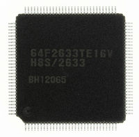
R5F61668RN50FPV Renesas Electronics America, R5F61668RN50FPV Datasheet - Page 1075

R5F61668RN50FPV
Manufacturer Part Number
R5F61668RN50FPV
Description
IC H8SX/1668 MCU FLASH 144LQFP
Manufacturer
Renesas Electronics America
Series
H8® H8SX/1600r
Datasheet
1.R5F61668RN50FPV.pdf
(1506 pages)
Specifications of R5F61668RN50FPV
Core Processor
H8SX
Core Size
16/32-Bit
Speed
50MHz
Connectivity
EBI/EMI, I²C, IrDA, SCI, SmartCard, USB
Peripherals
DMA, LVD, POR, PWM, WDT
Number Of I /o
92
Program Memory Size
1MB (1M x 8)
Program Memory Type
FLASH
Ram Size
56K x 8
Voltage - Supply (vcc/vdd)
3 V ~ 3.6 V
Data Converters
A/D 8x10b; D/A 2x8b
Oscillator Type
External
Operating Temperature
-20°C ~ 75°C
Package / Case
144-LQFP
For Use With
R0K561668S000BE - KIT STARTER FOR H8SX/1668R0K561664S001BE - KIT STARTER FOR H8SX/1651HS0005KCU11H - EMULATOR E10A-USB H8S(X),SH2(A)
Lead Free Status / RoHS Status
Lead free / RoHS Compliant
Eeprom Size
-
Available stocks
Company
Part Number
Manufacturer
Quantity
Price
Company:
Part Number:
R5F61668RN50FPV
Manufacturer:
Renesas Electronics America
Quantity:
10 000
- Current page: 1075 of 1506
- Download datasheet (9Mb)
21.3.3
ICMR selects MSB first or LSB first, controls the master mode wait and selects the number of
transfer bits.
Bit
7
6
5
4
3
Bit
Bit Name
Initial Value
R/W
I
Bit Name
WAIT
BCWP
2
C Bus Mode Register (ICMR)
R/W
7
0
Initial
Value
0
0
1
1
1
WAIT
R/W
6
0
R/W
R/W
R/W
R/W
5
1
Description
Reserved
The write value should always be 0.
Wait Insertion
This bit selects whether to insert a wait after data
transfer except for the acknowledge bit. When this bit is
set to 1, after the falling of the clock for the last data bit,
the low period is extended for two transfer clocks.
When this bit is cleared to 0, data and the acknowledge
bit are transferred consecutively with no waits inserted.
The setting of this bit is invalid in slave mode.
Reserved
These bits are always read as 1.
BC Write Protect
This bit controls the modification of the BC2 to BC0
bits. When modifying, this bit should be cleared to 0
and the MOV instruction should be used.
0: When writing, the values of BC2 to BC0 are set
1: When reading, 1 is always read
When writing, the settings of BC2 to BC0 are invalid.
4
1
BCWP
R/W
Rev. 2.00 Sep. 24, 2008 Page 1041 of 1468
3
1
Section 21 I
BC2
R/W
2
0
2
C Bus Interface 2 (IIC2)
BC1
R/W
1
0
REJ09B0412-0200
BC0
R/W
0
0
Related parts for R5F61668RN50FPV
Image
Part Number
Description
Manufacturer
Datasheet
Request
R

Part Number:
Description:
KIT STARTER FOR M16C/29
Manufacturer:
Renesas Electronics America
Datasheet:

Part Number:
Description:
KIT STARTER FOR R8C/2D
Manufacturer:
Renesas Electronics America
Datasheet:

Part Number:
Description:
R0K33062P STARTER KIT
Manufacturer:
Renesas Electronics America
Datasheet:

Part Number:
Description:
KIT STARTER FOR R8C/23 E8A
Manufacturer:
Renesas Electronics America
Datasheet:

Part Number:
Description:
KIT STARTER FOR R8C/25
Manufacturer:
Renesas Electronics America
Datasheet:

Part Number:
Description:
KIT STARTER H8S2456 SHARPE DSPLY
Manufacturer:
Renesas Electronics America
Datasheet:

Part Number:
Description:
KIT STARTER FOR R8C38C
Manufacturer:
Renesas Electronics America
Datasheet:

Part Number:
Description:
KIT STARTER FOR R8C35C
Manufacturer:
Renesas Electronics America
Datasheet:

Part Number:
Description:
KIT STARTER FOR R8CL3AC+LCD APPS
Manufacturer:
Renesas Electronics America
Datasheet:

Part Number:
Description:
KIT STARTER FOR RX610
Manufacturer:
Renesas Electronics America
Datasheet:

Part Number:
Description:
KIT STARTER FOR R32C/118
Manufacturer:
Renesas Electronics America
Datasheet:

Part Number:
Description:
KIT DEV RSK-R8C/26-29
Manufacturer:
Renesas Electronics America
Datasheet:

Part Number:
Description:
KIT STARTER FOR SH7124
Manufacturer:
Renesas Electronics America
Datasheet:

Part Number:
Description:
KIT STARTER FOR H8SX/1622
Manufacturer:
Renesas Electronics America
Datasheet:

Part Number:
Description:
KIT DEV FOR SH7203
Manufacturer:
Renesas Electronics America
Datasheet:


