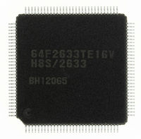
R5F61668RN50FPV Renesas Electronics America, R5F61668RN50FPV Datasheet - Page 1408

R5F61668RN50FPV
Manufacturer Part Number
R5F61668RN50FPV
Description
IC H8SX/1668 MCU FLASH 144LQFP
Manufacturer
Renesas Electronics America
Series
H8® H8SX/1600r
Datasheet
1.R5F61668RN50FPV.pdf
(1506 pages)
Specifications of R5F61668RN50FPV
Core Processor
H8SX
Core Size
16/32-Bit
Speed
50MHz
Connectivity
EBI/EMI, I²C, IrDA, SCI, SmartCard, USB
Peripherals
DMA, LVD, POR, PWM, WDT
Number Of I /o
92
Program Memory Size
1MB (1M x 8)
Program Memory Type
FLASH
Ram Size
56K x 8
Voltage - Supply (vcc/vdd)
3 V ~ 3.6 V
Data Converters
A/D 8x10b; D/A 2x8b
Oscillator Type
External
Operating Temperature
-20°C ~ 75°C
Package / Case
144-LQFP
For Use With
R0K561668S000BE - KIT STARTER FOR H8SX/1668R0K561664S001BE - KIT STARTER FOR H8SX/1651HS0005KCU11H - EMULATOR E10A-USB H8S(X),SH2(A)
Lead Free Status / RoHS Status
Lead free / RoHS Compliant
Eeprom Size
-
Available stocks
Company
Part Number
Manufacturer
Quantity
Price
Company:
Part Number:
R5F61668RN50FPV
Manufacturer:
Renesas Electronics America
Quantity:
10 000
- Current page: 1408 of 1506
- Download datasheet (9Mb)
Section 30 Electrical Characteristics
Table 30.8 Bus Timing (3)
Conditions: V
Rev. 2.00 Sep. 24, 2008 Page 1374 of 1468
REJ09B0412-0200
Item
CS delay time 2
CS delay time 3
Read data access time 1
Read data access time 3
Read data access time 7
Read data access time 8
Write data hold time 2
Read command setup time 1
Read command setup time 2
Read command hold time
Write command setup time 1
Write command setup time 2
Write command hold time 1
Write command hold time 2
CAS delay time 1
CAS delay time 2
CAS setup time 1
CAS setup time 2
CAS pulse width 1
CAS pulse width 2
CAS precharge time 1
CAS precharge time 2
OE delay time 1
OE delay time 2
Precharge time 1
Precharge time 2
AV
T
T
a
a
CC
= –20°C to +75°C (regular specifications),
= –40°C to +85°C (wide-range specifications)
CC
= PLLV
, V
SS
= PLLV
CC
= DrV
SS
Symbol
t
t
t
t
t
t
t
t
t
t
t
t
t
t
t
t
t
t
t
t
t
t
t
t
t
t
= DrV
CSD3
CSD4
AC1
AC3
AC7
AC8
WDH2
RCS1
RCS2
RCH
WCS1
WCS2
WCH1
WCH2
CASD1
CASD2
CSR1
CSR2
CASW1
CASW2
CPW1
CPW2
OED1
OED2
PCH1
PCH2
CC
= 3.0 V to 3.6 V*, AV
SS
= AV
Min.
1.0 × t
1.5 × t
2.0 × t
0.5 × t
0.5 × t
1.0 × t
0.5 × t
1.0 × t
0.5 × t
1.5 × t
1.0 × t
1.5 × t
1.0 × t
1.5 × t
1.0 × t
1.5 × t
SS
= 0 V, Bφ = 8 MHz to 50 MHz,
cyc
cyc
cyc
cyc
cyc
cyc
cyc
cyc
cyc
cyc
cyc
cyc
cyc
cyc
cyc
cyc
– 8
– 10
– 10
– 10
– 10
– 10
– 10
– 10
– 10
– 10
– 15
– 15
– 15
– 15
– 20
– 20
CC
Max.
15
15
1.0 × t
2.0 × t
4.0 × t
3.0 × t
15
15
15
15
= 3.0 V to 3.6 V, V
cyc
cyc
cyc
cyc
– 20 ns
– 20 ns
– 20 ns
– 20 ns
Unit
ns
ns
ns
ns
ns
ns
ns
ns
ns
ns
ns
ns
ns
ns
ns
ns
ns
ns
ns
ns
ns
ns
ref
Test
Conditions
Figures 30.19
to 30.28
= 3.0 V to
Related parts for R5F61668RN50FPV
Image
Part Number
Description
Manufacturer
Datasheet
Request
R

Part Number:
Description:
KIT STARTER FOR M16C/29
Manufacturer:
Renesas Electronics America
Datasheet:

Part Number:
Description:
KIT STARTER FOR R8C/2D
Manufacturer:
Renesas Electronics America
Datasheet:

Part Number:
Description:
R0K33062P STARTER KIT
Manufacturer:
Renesas Electronics America
Datasheet:

Part Number:
Description:
KIT STARTER FOR R8C/23 E8A
Manufacturer:
Renesas Electronics America
Datasheet:

Part Number:
Description:
KIT STARTER FOR R8C/25
Manufacturer:
Renesas Electronics America
Datasheet:

Part Number:
Description:
KIT STARTER H8S2456 SHARPE DSPLY
Manufacturer:
Renesas Electronics America
Datasheet:

Part Number:
Description:
KIT STARTER FOR R8C38C
Manufacturer:
Renesas Electronics America
Datasheet:

Part Number:
Description:
KIT STARTER FOR R8C35C
Manufacturer:
Renesas Electronics America
Datasheet:

Part Number:
Description:
KIT STARTER FOR R8CL3AC+LCD APPS
Manufacturer:
Renesas Electronics America
Datasheet:

Part Number:
Description:
KIT STARTER FOR RX610
Manufacturer:
Renesas Electronics America
Datasheet:

Part Number:
Description:
KIT STARTER FOR R32C/118
Manufacturer:
Renesas Electronics America
Datasheet:

Part Number:
Description:
KIT DEV RSK-R8C/26-29
Manufacturer:
Renesas Electronics America
Datasheet:

Part Number:
Description:
KIT STARTER FOR SH7124
Manufacturer:
Renesas Electronics America
Datasheet:

Part Number:
Description:
KIT STARTER FOR H8SX/1622
Manufacturer:
Renesas Electronics America
Datasheet:

Part Number:
Description:
KIT DEV FOR SH7203
Manufacturer:
Renesas Electronics America
Datasheet:


