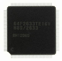
R5F61668RN50FPV Renesas Electronics America, R5F61668RN50FPV Datasheet - Page 1012

R5F61668RN50FPV
Manufacturer Part Number
R5F61668RN50FPV
Description
IC H8SX/1668 MCU FLASH 144LQFP
Manufacturer
Renesas Electronics America
Series
H8® H8SX/1600r
Datasheet
1.R5F61668RN50FPV.pdf
(1506 pages)
Specifications of R5F61668RN50FPV
Core Processor
H8SX
Core Size
16/32-Bit
Speed
50MHz
Connectivity
EBI/EMI, I²C, IrDA, SCI, SmartCard, USB
Peripherals
DMA, LVD, POR, PWM, WDT
Number Of I /o
92
Program Memory Size
1MB (1M x 8)
Program Memory Type
FLASH
Ram Size
56K x 8
Voltage - Supply (vcc/vdd)
3 V ~ 3.6 V
Data Converters
A/D 8x10b; D/A 2x8b
Oscillator Type
External
Operating Temperature
-20°C ~ 75°C
Package / Case
144-LQFP
For Use With
R0K561668S000BE - KIT STARTER FOR H8SX/1668R0K561664S001BE - KIT STARTER FOR H8SX/1651HS0005KCU11H - EMULATOR E10A-USB H8S(X),SH2(A)
Lead Free Status / RoHS Status
Lead free / RoHS Compliant
Eeprom Size
-
Available stocks
Company
Part Number
Manufacturer
Quantity
Price
Company:
Part Number:
R5F61668RN50FPV
Manufacturer:
Renesas Electronics America
Quantity:
10 000
- Current page: 1012 of 1506
- Download datasheet (9Mb)
Section 20 USB Function Module (USB)
20.3.10 EP0i Data Register (EPDR0i)
EPDR0i is an 8-byte transmit FIFO buffer for endpoint 0. EPDR0i holds one packet of transmit
data for control-in. Transmit data is fixed by writing one packet of data and setting EP0iPKTE in
the trigger register. When an ACK handshake is returned from the host after the data has been
transmitted, EP0iTS in interrupt flag register 0 is set. This FIFO buffer can be initialized by means
of EP0iCLR in the FCLR register.
Rev. 2.00 Sep. 24, 2008 Page 978 of 1468
REJ09B0412-0200
Bit
7
6, 5
4
3
2
1
0
Bit
7 to 0
Bit
Bit Name
Initial Value
R/W
Bit Name
SSRSME
SURSE
CFDN
SETCE
SETIE
Bit Name
D7 to D0
Undefined
D7
W
7
Undefined
0
0
0
0
Initial
Value
All 0
0
0
Initial
Value
Undefined W
D6
W
6
Undefined
R/W
R/W
R/W
R/W
R/W
R
R/W
R/W
R/W
D5
W
5
Description
Resume Detection for Software Standby Cancel
For the details of the operation, see section 20.5.3,
Suspend and Resume Operations.
Reserved
These bits are always read as 0. The write value
should always be 0.
Suspend/Resume Detection
For the details of the operation, see section 20.5.3,
Suspend and Resume Operations.
End Point Information Load End
Reserved
This bit is always read as 0. The write value should
always be 0.
Set_Configuration Command Detection
Set_Interface Command Detection
Description
Data register for control-in transfer
Undefined
D4
W
4
Undefined
D3
W
3
Undefined
D2
W
2
Undefined
D1
W
1
Undefined
D0
W
0
Related parts for R5F61668RN50FPV
Image
Part Number
Description
Manufacturer
Datasheet
Request
R

Part Number:
Description:
KIT STARTER FOR M16C/29
Manufacturer:
Renesas Electronics America
Datasheet:

Part Number:
Description:
KIT STARTER FOR R8C/2D
Manufacturer:
Renesas Electronics America
Datasheet:

Part Number:
Description:
R0K33062P STARTER KIT
Manufacturer:
Renesas Electronics America
Datasheet:

Part Number:
Description:
KIT STARTER FOR R8C/23 E8A
Manufacturer:
Renesas Electronics America
Datasheet:

Part Number:
Description:
KIT STARTER FOR R8C/25
Manufacturer:
Renesas Electronics America
Datasheet:

Part Number:
Description:
KIT STARTER H8S2456 SHARPE DSPLY
Manufacturer:
Renesas Electronics America
Datasheet:

Part Number:
Description:
KIT STARTER FOR R8C38C
Manufacturer:
Renesas Electronics America
Datasheet:

Part Number:
Description:
KIT STARTER FOR R8C35C
Manufacturer:
Renesas Electronics America
Datasheet:

Part Number:
Description:
KIT STARTER FOR R8CL3AC+LCD APPS
Manufacturer:
Renesas Electronics America
Datasheet:

Part Number:
Description:
KIT STARTER FOR RX610
Manufacturer:
Renesas Electronics America
Datasheet:

Part Number:
Description:
KIT STARTER FOR R32C/118
Manufacturer:
Renesas Electronics America
Datasheet:

Part Number:
Description:
KIT DEV RSK-R8C/26-29
Manufacturer:
Renesas Electronics America
Datasheet:

Part Number:
Description:
KIT STARTER FOR SH7124
Manufacturer:
Renesas Electronics America
Datasheet:

Part Number:
Description:
KIT STARTER FOR H8SX/1622
Manufacturer:
Renesas Electronics America
Datasheet:

Part Number:
Description:
KIT DEV FOR SH7203
Manufacturer:
Renesas Electronics America
Datasheet:


