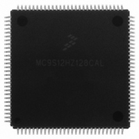
MC9S12HZ128CAL Freescale Semiconductor, MC9S12HZ128CAL Datasheet - Page 655

MC9S12HZ128CAL
Manufacturer Part Number
MC9S12HZ128CAL
Description
IC MCU 16BIT 128K FLASH 112-LQFP
Manufacturer
Freescale Semiconductor
Series
HCS12r
Datasheet
1.MC9S12HZ128CAL.pdf
(692 pages)
Specifications of MC9S12HZ128CAL
Core Processor
HCS12
Core Size
16-Bit
Speed
25MHz
Connectivity
CAN, EBI/EMI, I²C, SCI, SPI
Peripherals
LCD, Motor control PWM, POR, PWM, WDT
Number Of I /o
85
Program Memory Size
128KB (128K x 8)
Program Memory Type
FLASH
Eeprom Size
2K x 8
Ram Size
6K x 8
Voltage - Supply (vcc/vdd)
2.35 V ~ 5.5 V
Data Converters
A/D 16x10b
Oscillator Type
Internal
Operating Temperature
-40°C ~ 85°C
Package / Case
112-LQFP
Processor Series
S12H
Core
HCS12
Data Bus Width
16 bit
Data Ram Size
6 KB
Interface Type
I2C, SCI, SPI
Maximum Clock Frequency
50 MHz
Number Of Programmable I/os
85
Number Of Timers
8
Maximum Operating Temperature
+ 85 C
Mounting Style
SMD/SMT
3rd Party Development Tools
EWHCS12
Minimum Operating Temperature
- 40 C
On-chip Adc
10 bit, 16 Channel
Lead Free Status / RoHS Status
Lead free / RoHS Compliant
Available stocks
Company
Part Number
Manufacturer
Quantity
Price
Company:
Part Number:
MC9S12HZ128CAL
Manufacturer:
Freescale Semiconductor
Quantity:
10 000
- Current page: 655 of 692
- Download datasheet (4Mb)
Appendix B
PCB Layout Guidelines
The PCB must be carefully laid out to ensure proper operation of the voltage regulator as well as of the
MCU itself. The following rules must be observed:
Example layouts are illustrated on
Freescale Semiconductor
•
•
•
•
•
•
•
Every supply pair must be decoupled by a ceramic/tantalum capacitor connected as near as
possible to the corresponding pins (C1–C9).
Central point of the ground star should be the V
Use low ohmic low inductance connections between V
V
Keep traces of V
C11, C14 and Q1 as small as possible.
Do not place other signals or supplies underneath area occupied by C10, C11, C14 and Q1 and the
connection area to the MCU.
Central power input should be fed in at the V
SSPLL
must be directly connected to V
Component
C10
C11
C12
C13
C14
C1
C2
C3
C4
C5
C6
C7
C8
C9
R1
Q1
SSPLL
, EXTAL and XTAL as short as possible and occupied board area for C10,
Table B-1. Recommended Components
Figure B-1
PLL loop filter cap
PLL loop filter cap
Quartz/Resonator
PLL loop filter res
V
V
V
V
V
V
MC9S12HZ256 Data Sheet, Rev. 2.05
V
V
V
OSC load cap
OSC load cap
DC cutoff cap
DDPLL
DDM3
DDM2
DDM1
DDX2
DDX1
DDR
DDA
DD1
Purpose
filter cap
filter cap
filter cap
filter cap
filter cap
filter cap
filter cap
filter cap
filter cap
and
SS1
Figure
.
DDA
SS1
X7R/tantalum
X7R/tantalum
X7R/tantalum
X7R/tantalum
X7R/tantalum
X7R/tantalum
X7R/tantalum
ceramic X7R
ceramic X7R
/V
See CRG block description chapter
B-2.
pin.
SSA
Type
SS1
pins.
, V
SS2
, V
SSA
100 nF .. 220 nF
100 .. 220 nF
Appendix B PCB Layout Guidelines
>=100 nF
>=100 nF
>=100 nF
>=100 nF
>=100 nF
>=100 nF
>=100 nF
, V
Value
SSX1,2
and V
SSM1,2,3
655
.
Related parts for MC9S12HZ128CAL
Image
Part Number
Description
Manufacturer
Datasheet
Request
R
Part Number:
Description:
Manufacturer:
Freescale Semiconductor, Inc
Datasheet:
Part Number:
Description:
Manufacturer:
Freescale Semiconductor, Inc
Datasheet:
Part Number:
Description:
Manufacturer:
Freescale Semiconductor, Inc
Datasheet:
Part Number:
Description:
Manufacturer:
Freescale Semiconductor, Inc
Datasheet:
Part Number:
Description:
Manufacturer:
Freescale Semiconductor, Inc
Datasheet:
Part Number:
Description:
Manufacturer:
Freescale Semiconductor, Inc
Datasheet:
Part Number:
Description:
Manufacturer:
Freescale Semiconductor, Inc
Datasheet:
Part Number:
Description:
Manufacturer:
Freescale Semiconductor, Inc
Datasheet:
Part Number:
Description:
Manufacturer:
Freescale Semiconductor, Inc
Datasheet:
Part Number:
Description:
Manufacturer:
Freescale Semiconductor, Inc
Datasheet:
Part Number:
Description:
Manufacturer:
Freescale Semiconductor, Inc
Datasheet:
Part Number:
Description:
Manufacturer:
Freescale Semiconductor, Inc
Datasheet:
Part Number:
Description:
Manufacturer:
Freescale Semiconductor, Inc
Datasheet:
Part Number:
Description:
Manufacturer:
Freescale Semiconductor, Inc
Datasheet:
Part Number:
Description:
Manufacturer:
Freescale Semiconductor, Inc
Datasheet:


