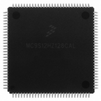
MC9S12HZ128CAL Freescale Semiconductor, MC9S12HZ128CAL Datasheet - Page 626

MC9S12HZ128CAL
Manufacturer Part Number
MC9S12HZ128CAL
Description
IC MCU 16BIT 128K FLASH 112-LQFP
Manufacturer
Freescale Semiconductor
Series
HCS12r
Datasheet
1.MC9S12HZ128CAL.pdf
(692 pages)
Specifications of MC9S12HZ128CAL
Core Processor
HCS12
Core Size
16-Bit
Speed
25MHz
Connectivity
CAN, EBI/EMI, I²C, SCI, SPI
Peripherals
LCD, Motor control PWM, POR, PWM, WDT
Number Of I /o
85
Program Memory Size
128KB (128K x 8)
Program Memory Type
FLASH
Eeprom Size
2K x 8
Ram Size
6K x 8
Voltage - Supply (vcc/vdd)
2.35 V ~ 5.5 V
Data Converters
A/D 16x10b
Oscillator Type
Internal
Operating Temperature
-40°C ~ 85°C
Package / Case
112-LQFP
Processor Series
S12H
Core
HCS12
Data Bus Width
16 bit
Data Ram Size
6 KB
Interface Type
I2C, SCI, SPI
Maximum Clock Frequency
50 MHz
Number Of Programmable I/os
85
Number Of Timers
8
Maximum Operating Temperature
+ 85 C
Mounting Style
SMD/SMT
3rd Party Development Tools
EWHCS12
Minimum Operating Temperature
- 40 C
On-chip Adc
10 bit, 16 Channel
Lead Free Status / RoHS Status
Lead free / RoHS Compliant
Available stocks
Company
Part Number
Manufacturer
Quantity
Price
Company:
Part Number:
MC9S12HZ128CAL
Manufacturer:
Freescale Semiconductor
Quantity:
10 000
- Current page: 626 of 692
- Download datasheet (4Mb)
Appendix A Electrical Characteristics
A.1.6
All ESD testing is in conformity with CDF-AEC-Q100 Stress test qualification for Automotive Grade
Integrated Circuits. During the device qualification ESD stresses were performed for the Human Body
Model (HBM), the Machine Model (MM) and the Charge Device Model.
A device will be defined as a failure if after exposure to ESD pulses the device no longer meets the device
specification. Complete DC parametric and functional testing is performed per the applicable device
specification at room temperature followed by hot temperature, unless specified otherwise in the device
specification.
626
2
3
4
5
6
Num C
The device contains an internal voltage regulator to generate the logic and PLL supply out of the I/O supply. The
absolute maximum ratings apply when the device is powered from an external source.
All digital I/O pins are internally clamped to V
Ports PU and PV are internally clamped to V
Those pins are internally clamped to V
This pin is clamped low to V
1
2
3
Human Body
Machine
Latch-up
ESD Protection and Latch-up Immunity
C Human Body Model (HBM)
C Machine Model (MM)
C Charge Device Model (CDM)
Model
Series Resistance
Storage Capacitance
Number of Pulse per pin
positive
negative
Series Resistance
Storage Capacitance
Number of Pulse per pin
positive
negative
Minimum input voltage limit
Maximum input voltage limit
Table A-3. ESD and Latch-Up Protection Characteristics
Table A-2. ESD and Latch-up Test Conditions
SSPLL
Rating
, but not clamped high. This pin must be tied low in applications.
MC9S12HZ256 Data Sheet, Rev. 2.05
SSPLL
Description
SSM
and V
SSX1/2
and V
DDPLL
and V
DDM
.
DDX1/2
.
, V
Symbol
V
V
V
SSM
HBM
CDM
MM
and V
Symbol
DDM
R1
R1
C
C
–
–
2000
Min
200
500
or V
SSA
Value
and V
1500
–2.5
100
200
7.5
–
3
3
0
–
3
3
Freescale Semiconductor
Max
–
–
–
DDA
.
Unit
pF
pF
W
W
V
V
Unit
V
V
V
Related parts for MC9S12HZ128CAL
Image
Part Number
Description
Manufacturer
Datasheet
Request
R
Part Number:
Description:
Manufacturer:
Freescale Semiconductor, Inc
Datasheet:
Part Number:
Description:
Manufacturer:
Freescale Semiconductor, Inc
Datasheet:
Part Number:
Description:
Manufacturer:
Freescale Semiconductor, Inc
Datasheet:
Part Number:
Description:
Manufacturer:
Freescale Semiconductor, Inc
Datasheet:
Part Number:
Description:
Manufacturer:
Freescale Semiconductor, Inc
Datasheet:
Part Number:
Description:
Manufacturer:
Freescale Semiconductor, Inc
Datasheet:
Part Number:
Description:
Manufacturer:
Freescale Semiconductor, Inc
Datasheet:
Part Number:
Description:
Manufacturer:
Freescale Semiconductor, Inc
Datasheet:
Part Number:
Description:
Manufacturer:
Freescale Semiconductor, Inc
Datasheet:
Part Number:
Description:
Manufacturer:
Freescale Semiconductor, Inc
Datasheet:
Part Number:
Description:
Manufacturer:
Freescale Semiconductor, Inc
Datasheet:
Part Number:
Description:
Manufacturer:
Freescale Semiconductor, Inc
Datasheet:
Part Number:
Description:
Manufacturer:
Freescale Semiconductor, Inc
Datasheet:
Part Number:
Description:
Manufacturer:
Freescale Semiconductor, Inc
Datasheet:
Part Number:
Description:
Manufacturer:
Freescale Semiconductor, Inc
Datasheet:


