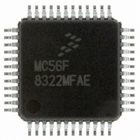
MC56F8322MFAE Freescale Semiconductor, MC56F8322MFAE Datasheet - Page 95

MC56F8322MFAE
Manufacturer Part Number
MC56F8322MFAE
Description
IC DSP 16BIT 60MHZ 48-LQFP
Manufacturer
Freescale Semiconductor
Series
56F8xxxr
Datasheet
1.MC56F8122VFAE.pdf
(136 pages)
Specifications of MC56F8322MFAE
Core Processor
56800
Core Size
16-Bit
Speed
60MHz
Connectivity
CAN, SCI, SPI
Peripherals
POR, PWM, Temp Sensor, WDT
Number Of I /o
21
Program Memory Size
40KB (20K x 16)
Program Memory Type
FLASH
Ram Size
6K x 16
Voltage - Supply (vcc/vdd)
2.25 V ~ 3.6 V
Data Converters
A/D 6x12b
Oscillator Type
Internal
Operating Temperature
-40°C ~ 125°C
Package / Case
48-LQFP
Cpu Family
56F8xxx
Device Core Size
16b
Frequency (max)
60MHz
Interface Type
CAN/SCI/SPI
Total Internal Ram Size
4KB
# I/os (max)
21
Number Of Timers - General Purpose
2
Operating Supply Voltage (typ)
2.5/3.3V
Operating Supply Voltage (max)
2.75/3.6V
Operating Supply Voltage (min)
2.25/3V
On-chip Adc
2(3-chx12-bit)
Instruction Set Architecture
CISC
Operating Temp Range
-40C to 125C
Operating Temperature Classification
Automotive
Mounting
Surface Mount
Pin Count
48
Package Type
LQFP
Data Bus Width
16 bit
Processor Series
MC56F83xx
Core
56800E
Numeric And Arithmetic Format
Fixed-Point
Device Million Instructions Per Second
40 MIPs
Maximum Clock Frequency
60 MHz
Number Of Programmable I/os
21
Data Ram Size
4 KB
Operating Supply Voltage
- 0.3 V to + 4 V
Maximum Operating Temperature
+ 125 C
Mounting Style
SMD/SMT
Data Rom Size
8 KB
Minimum Operating Temperature
- 40 C
For Use With
MC56F8323EVME - BOARD EVALUATION MC56F8323
Lead Free Status / RoHS Status
Lead free / RoHS Compliant
Eeprom Size
-
Lead Free Status / Rohs Status
Compliant
Available stocks
Company
Part Number
Manufacturer
Quantity
Price
Company:
Part Number:
MC56F8322MFAE
Manufacturer:
VISHAY
Quantity:
12 500
Company:
Part Number:
MC56F8322MFAE
Manufacturer:
Freescale Semiconductor
Quantity:
10 000
Part Number:
MC56F8322MFAE
Manufacturer:
FREESCALE
Quantity:
20 000
Part 7 Security Features
The 56F8322/56F8122 offer security features intended to prevent unauthorized users from reading the
contents of the Flash Memory (FM) array. The Flash security consists of several hardware interlocks that
block the means by which an unauthorized user could gain access to the Flash array.
However, part of the security must lie with the user’s code. An extreme example would be user’s code that
dumps the contents of the internal program, as this code would defeat the purpose of security. At the same
time, the user may also wish to put a “backdoor” in his program. As an example, the user downloads a
security key through the SCI, allowing access to a programming routine that updates parameters stored in
another section of the Flash.
7.1 Operation with Security Enabled
Once the user has programmed the Flash with his application code, the device can be secured by
programming the security bytes located in the FM configuration field, which occupies a portion of the FM
array. These non-volatile bytes will keep the part secured through reset and through power-down of the
device. Only two bytes within this field are used to enable or disable security. Refer to the Flash Memory
chapter in the 56F8300 Peripheral User Manual for the state of the security bytes and the resulting state
of security. When Flash security mode is enabled in accordance with the method described in the Flash
Memory module specification, the device will disable the core EOnCE debug capabilities. Normal
program execution is otherwise unaffected.
7.2 Flash Access Blocking Mechanisms
The 56F8322/56F8122 have several operating functional and test modes. Effective Flash security must
address operating mode selection and anticipate modes in which the on-chip Flash can be compromised
and read without explicit user permission. Methods to block these are outlined in the next subsections.
7.2.1
At boot time, the SIM determines in which functional modes the device will operate. These are:
When Flash security is enabled as described in the Flash Memory module specification, the device will
disable the EOnCE debug interface.
7.2.2
On-chip Flash can be read by issuing commands across the EOnCE port, which is the debug interface for
the 56800E CPU. The TRST, TCLK, TMS, TDO, and TDI pins comprise a JTAG interface onto which
the EOnCE port functionality is mapped. When the device boots, the chip-level JTAG TAP (Test Access
Port) is active and provides the chip’s boundary scan capability and access to the ID register.
Freescale Semiconductor
Preliminary
•
•
Unsecured Mode
Secure Mode (EOnCE disabled)
Forced Operating Mode Selection
Disabling EOnCE Access
56F8322 Technical Data, Rev. 16
Operation with Security Enabled
95


