MC56F8322MFAE Freescale Semiconductor, MC56F8322MFAE Datasheet - Page 89
MC56F8322MFAE
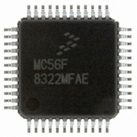
Manufacturer Part Number
MC56F8322MFAE
Description
IC DSP 16BIT 60MHZ 48-LQFP
Manufacturer
Freescale Semiconductor
Series
56F8xxxr
Datasheet
1.MC56F8122VFAE.pdf
(136 pages)
Specifications of MC56F8322MFAE
Core Processor
56800
Core Size
16-Bit
Speed
60MHz
Connectivity
CAN, SCI, SPI
Peripherals
POR, PWM, Temp Sensor, WDT
Number Of I /o
21
Program Memory Size
40KB (20K x 16)
Program Memory Type
FLASH
Ram Size
6K x 16
Voltage - Supply (vcc/vdd)
2.25 V ~ 3.6 V
Data Converters
A/D 6x12b
Oscillator Type
Internal
Operating Temperature
-40°C ~ 125°C
Package / Case
48-LQFP
Cpu Family
56F8xxx
Device Core Size
16b
Frequency (max)
60MHz
Interface Type
CAN/SCI/SPI
Total Internal Ram Size
4KB
# I/os (max)
21
Number Of Timers - General Purpose
2
Operating Supply Voltage (typ)
2.5/3.3V
Operating Supply Voltage (max)
2.75/3.6V
Operating Supply Voltage (min)
2.25/3V
On-chip Adc
2(3-chx12-bit)
Instruction Set Architecture
CISC
Operating Temp Range
-40C to 125C
Operating Temperature Classification
Automotive
Mounting
Surface Mount
Pin Count
48
Package Type
LQFP
Data Bus Width
16 bit
Processor Series
MC56F83xx
Core
56800E
Numeric And Arithmetic Format
Fixed-Point
Device Million Instructions Per Second
40 MIPs
Maximum Clock Frequency
60 MHz
Number Of Programmable I/os
21
Data Ram Size
4 KB
Operating Supply Voltage
- 0.3 V to + 4 V
Maximum Operating Temperature
+ 125 C
Mounting Style
SMD/SMT
Data Rom Size
8 KB
Minimum Operating Temperature
- 40 C
For Use With
MC56F8323EVME - BOARD EVALUATION MC56F8323
Lead Free Status / RoHS Status
Lead free / RoHS Compliant
Eeprom Size
-
Lead Free Status / Rohs Status
Compliant
Available stocks
Company
Part Number
Manufacturer
Quantity
Price
Company:

Part Number:
MC56F8322MFAE
Manufacturer:
VISHAY
Quantity:
12 500
Company:
Part Number:
MC56F8322MFAE
Manufacturer:
Freescale Semiconductor
Quantity:
10 000
Part Number:
MC56F8322MFAE
Manufacturer:
FREESCALE
Quantity:
20 000


6.5.8.4
This bit selects the alternate function for GPIOB1.
6.5.8.5
This bit selects the alternate function for GPIOB0.
6.5.8.6
This bit selects the alternate function for GPIOA5.
6.5.8.7
This bit selects the alternate function for GPIOA4.
6.5.8.8
This bit selects the alternate function for GPIOA3.
6.5.8.9
This bit selects the alternate function for GPIOA2.
6.5.9
The Peripheral Clock Enable register is used to enable or disable clocks to the peripherals as a power
savings feature. The clocks can be individually controlled for each peripheral on the chip.
Freescale Semiconductor
Preliminary
•
•
•
•
•
•
•
•
•
•
•
•
Base + $C
RESET
Read
Write
0 = MISO0 (default)
1 = RXD1
0 = SS0 (default)
1 = TXD1
0 = PWMA5
1 = SCLK1
0 = PWMA4
1 = MOS1
0 = PWMA3
1 = MISO1
0 = PWMA2
1 = SS1
Peripheral Clock Enable Register (SIM_PCE)
GPIOB1 (B1)—Bit 5
GPIOB0 (B0)—Bit 4
GPIOA5 (A5)—Bit 3
GPIOA4 (A4)—Bit 2
GPIOA3 (A3)—Bit 1
GPIOA2 (A2)—Bit 0
15
1
1
Figure 6-12 Peripheral Clock Enable Register (SIM_PCE)
14
1
1
ADCA
13
1
CAN
12
1
11
1
1
56F8322 Technical Data, Rev. 16
DEC0
10
1
9
1
1
TMRC
8
1
7
1
1
TMRA SCI 1 SCI 0
6
1
5
1
4
1
SPI1
3
1
SPI0
2
1
Register Descriptions
1
1
1
PWMA
0
1
89
Related parts for MC56F8322MFAE
Image
Part Number
Description
Manufacturer
Datasheet
Request
R

Part Number:
Description:
Manufacturer:
Freescale Semiconductor, Inc
Datasheet:
Part Number:
Description:
Manufacturer:
Freescale Semiconductor, Inc
Datasheet:
Part Number:
Description:
Manufacturer:
Freescale Semiconductor, Inc
Datasheet:
Part Number:
Description:
Manufacturer:
Freescale Semiconductor, Inc
Datasheet:
Part Number:
Description:
Manufacturer:
Freescale Semiconductor, Inc
Datasheet:
Part Number:
Description:
Manufacturer:
Freescale Semiconductor, Inc
Datasheet:
Part Number:
Description:
Manufacturer:
Freescale Semiconductor, Inc
Datasheet:
Part Number:
Description:
Manufacturer:
Freescale Semiconductor, Inc
Datasheet:
Part Number:
Description:
Manufacturer:
Freescale Semiconductor, Inc
Datasheet:
Part Number:
Description:
Manufacturer:
Freescale Semiconductor, Inc
Datasheet:
Part Number:
Description:
Manufacturer:
Freescale Semiconductor, Inc
Datasheet:
Part Number:
Description:
Manufacturer:
Freescale Semiconductor, Inc
Datasheet:
Part Number:
Description:
Manufacturer:
Freescale Semiconductor, Inc
Datasheet:
Part Number:
Description:
Manufacturer:
Freescale Semiconductor, Inc
Datasheet:
Part Number:
Description:
Manufacturer:
Freescale Semiconductor, Inc
Datasheet: