MC56F8322MFAE Freescale Semiconductor, MC56F8322MFAE Datasheet - Page 6
MC56F8322MFAE
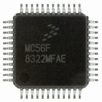
Manufacturer Part Number
MC56F8322MFAE
Description
IC DSP 16BIT 60MHZ 48-LQFP
Manufacturer
Freescale Semiconductor
Series
56F8xxxr
Datasheet
1.MC56F8122VFAE.pdf
(136 pages)
Specifications of MC56F8322MFAE
Core Processor
56800
Core Size
16-Bit
Speed
60MHz
Connectivity
CAN, SCI, SPI
Peripherals
POR, PWM, Temp Sensor, WDT
Number Of I /o
21
Program Memory Size
40KB (20K x 16)
Program Memory Type
FLASH
Ram Size
6K x 16
Voltage - Supply (vcc/vdd)
2.25 V ~ 3.6 V
Data Converters
A/D 6x12b
Oscillator Type
Internal
Operating Temperature
-40°C ~ 125°C
Package / Case
48-LQFP
Cpu Family
56F8xxx
Device Core Size
16b
Frequency (max)
60MHz
Interface Type
CAN/SCI/SPI
Total Internal Ram Size
4KB
# I/os (max)
21
Number Of Timers - General Purpose
2
Operating Supply Voltage (typ)
2.5/3.3V
Operating Supply Voltage (max)
2.75/3.6V
Operating Supply Voltage (min)
2.25/3V
On-chip Adc
2(3-chx12-bit)
Instruction Set Architecture
CISC
Operating Temp Range
-40C to 125C
Operating Temperature Classification
Automotive
Mounting
Surface Mount
Pin Count
48
Package Type
LQFP
Data Bus Width
16 bit
Processor Series
MC56F83xx
Core
56800E
Numeric And Arithmetic Format
Fixed-Point
Device Million Instructions Per Second
40 MIPs
Maximum Clock Frequency
60 MHz
Number Of Programmable I/os
21
Data Ram Size
4 KB
Operating Supply Voltage
- 0.3 V to + 4 V
Maximum Operating Temperature
+ 125 C
Mounting Style
SMD/SMT
Data Rom Size
8 KB
Minimum Operating Temperature
- 40 C
For Use With
MC56F8323EVME - BOARD EVALUATION MC56F8323
Lead Free Status / RoHS Status
Lead free / RoHS Compliant
Eeprom Size
-
Lead Free Status / Rohs Status
Compliant
Available stocks
Company
Part Number
Manufacturer
Quantity
Price
Company:

Part Number:
MC56F8322MFAE
Manufacturer:
VISHAY
Quantity:
12 500
Company:
Part Number:
MC56F8322MFAE
Manufacturer:
Freescale Semiconductor
Quantity:
10 000
Part Number:
MC56F8322MFAE
Manufacturer:
FREESCALE
Quantity:
20 000


6
Part 1: Overview . . . . . . . . . . . . . . . . . . . . . . 7
Part 2: Signal/Connection Descriptions . . 16
Part 3: On-Chip Clock Synthesis (OCCS) . 28
Part 4: Memory Map . . . . . . . . . . . . . . . . . . 32
Part 5: Interrupt Controller (ITCN) . . . . . . . 54
Part 6: System Integration Module (SIM) . . 79
Part 7: Security Features . . . . . . . . . . . . . . 95
1.1. 56F8322/56F8122 Features . . . . . . . . . . . . . 7
1.2. Device Description . . . . . . . . . . . . . . . . . . . . 9
1.3. Award-Winning Development Environment 10
1.4. Architecture Block Diagram . . . . . . . . . . . . . 11
1.5. Product Documentation . . . . . . . . . . . . . . . 15
1.6. Data Sheet Conventions . . . . . . . . . . . . . . . 15
2.1. Introduction . . . . . . . . . . . . . . . . . . . . . . . . . 16
2.2. Signal Pins . . . . . . . . . . . . . . . . . . . . . . . . . 19
3.1. Introduction . . . . . . . . . . . . . . . . . . . . . . . . . 28
3.2. External Clock Operation . . . . . . . . . . . . . . 28
3.3. Use of On-Chip Relaxation Oscillator . . . . . 30
3.4. Internal Clock Operation . . . . . . . . . . . . . . . 30
3.5. Registers . . . . . . . . . . . . . . . . . . . . . . . . . . . 31
4.1. Introduction . . . . . . . . . . . . . . . . . . . . . . . . . 32
4.2. Program Map . . . . . . . . . . . . . . . . . . . . . . . . 32
4.3. Interrupt Vector Table . . . . . . . . . . . . . . . . . 33
4.4. Data Map . . . . . . . . . . . . . . . . . . . . . . . . . . . 36
4.5. Flash Memory Map . . . . . . . . . . . . . . . . . . . 36
4.6. EOnCE Memory Map . . . . . . . . . . . . . . . . . 38
4.7. Peripheral Memory Mapped Registers . . . . 38
4.8. Factory-Programmed Memory . . . . . . . . . . 54
5.1. Introduction . . . . . . . . . . . . . . . . . . . . . . . . . 54
5.2. Features. . . . . . . . . . . . . . . . . . . . . . . . . . . . 54
5.3. Functional Description . . . . . . . . . . . . . . . . 54
5.4. Block Diagram . . . . . . . . . . . . . . . . . . . . . . . 56
5.5. Operating Modes . . . . . . . . . . . . . . . . . . . . 56
5.6. Register Descriptions . . . . . . . . . . . . . . . . . 57
5.7. Resets . . . . . . . . . . . . . . . . . . . . . . . . . . . . . 79
6.1. Introduction . . . . . . . . . . . . . . . . . . . . . . . . . 79
6.2. Features . . . . . . . . . . . . . . . . . . . . . . . . . . . 80
6.3. Operating Modes . . . . . . . . . . . . . . . . . . . . . 80
6.4. Operating Mode Register. . . . . . . . . . . . . . . 81
6.5. Register Descriptions. . . . . . . . . . . . . . . . . . 81
6.6. Clock Generation Overview . . . . . . . . . . . . . 93
6.7. Power-Down Modes. . . . . . . . . . . . . . . . . . . 93
6.8. Stop and Wait Mode Disable Function . . . . 94
6.9. Resets . . . . . . . . . . . . . . . . . . . . . . . . . . . . . 94
7.1. Operation with Security Enabled . . . . . . . . . 95
7.2. Flash Access Blocking Mechanisms . . . . . . 95
56F8322 Techncial Data, Rev. 16
Table of Contents
Part 8: General Purpose Input/Output
Part 9: Joint Test Action Group (JTAG) . . 100
Part 10: Specifications . . . . . . . . . . . . . . . . 101
Part 11: Packaging . . . . . . . . . . . . . . . . . . 126
Part 12: Design Considerations . . . . . . . . 131
Part 13: Ordering Information . . . . . . . . . 134
8.1. Introduction . . . . . . . . . . . . . . . . . . . . . . . . . 98
8.2. Configuration . . . . . . . . . . . . . . . . . . . . . . . . 98
8.3. Memory Maps . . . . . . . . . . . . . . . . . . . . . . .100
9.1. JTAG Information . . . . . . . . . . . . . . . . . . . 100
10.1. General Characteristics . . . . . . . . . . . . . .101
10.2. DC Electrical Characteristics . . . . . . . . . .105
10.3. AC Electrical Characteristics . . . . . . . . . .109
10.4. Flash Memory Characteristics . . . . . . . . . 110
10.5. External Clock Operation Timing . . . . . . .111
10.6. Phase Locked Loop Timing . . . . . . . . . . . 111
10.7. Oscillator Parameters . . . . . . . . . . . . . . . 112
10.8. Reset, Stop, Wait, Mode Select,
10.9. Serial Peripheral Interface (SPI) Timing . .115
10.10. Quad Timer Timing . . . . . . . . . . . . . . . . .118
10.11. Quadrature Decoder Timing . . . . . . . . . .118
10.12. Serial Communication Interface
10.13. Controller Area Network (CAN) Timing .120
10.14. JTAG Timing . . . . . . . . . . . . . . . . . . . . . .120
10.15. Analog-to-Digital Converter
10.16. Equivalent Circuit for ADC Inputs . . . . . .124
10.17. Power Consumption . . . . . . . . . . . . . . . 124
11.1. 56F8322 Package and
11.2. 56F8122 Package and Pin-Out
12.1. Thermal Design Considerations . . . . . . . 131
12.2. Electrical Design Considerations . . . . . . .132
12.3. Power Distribution and I/O Ring
(GPIO) . . . . . . . . . . . . . . . . . . . . . . . . 98
and Interrupt Timing . . . . . . . . . . 113
(SCI) Timing . . . . . . . . . . . . . . . . .119
(ADC) Parameters . . . . . . . . . . . .121
Pin-Out Information . . . . . . . . . . .126
Information . . . . . . . . . . . . . . . . . 128
Implementation . . . . . . . . . . . . . .133
Freescale Semiconductor
Preliminary
Related parts for MC56F8322MFAE
Image
Part Number
Description
Manufacturer
Datasheet
Request
R

Part Number:
Description:
Manufacturer:
Freescale Semiconductor, Inc
Datasheet:
Part Number:
Description:
Manufacturer:
Freescale Semiconductor, Inc
Datasheet:
Part Number:
Description:
Manufacturer:
Freescale Semiconductor, Inc
Datasheet:
Part Number:
Description:
Manufacturer:
Freescale Semiconductor, Inc
Datasheet:
Part Number:
Description:
Manufacturer:
Freescale Semiconductor, Inc
Datasheet:
Part Number:
Description:
Manufacturer:
Freescale Semiconductor, Inc
Datasheet:
Part Number:
Description:
Manufacturer:
Freescale Semiconductor, Inc
Datasheet:
Part Number:
Description:
Manufacturer:
Freescale Semiconductor, Inc
Datasheet:
Part Number:
Description:
Manufacturer:
Freescale Semiconductor, Inc
Datasheet:
Part Number:
Description:
Manufacturer:
Freescale Semiconductor, Inc
Datasheet:
Part Number:
Description:
Manufacturer:
Freescale Semiconductor, Inc
Datasheet:
Part Number:
Description:
Manufacturer:
Freescale Semiconductor, Inc
Datasheet:
Part Number:
Description:
Manufacturer:
Freescale Semiconductor, Inc
Datasheet:
Part Number:
Description:
Manufacturer:
Freescale Semiconductor, Inc
Datasheet:
Part Number:
Description:
Manufacturer:
Freescale Semiconductor, Inc
Datasheet: