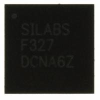
C8051F327-GM Silicon Laboratories Inc, C8051F327-GM Datasheet - Page 92

C8051F327-GM
Manufacturer Part Number
C8051F327-GM
Description
IC 8051 MCU FLASH 16K 28QFN
Manufacturer
Silicon Laboratories Inc
Series
C8051F32xr
Specifications of C8051F327-GM
Program Memory Type
FLASH
Program Memory Size
16KB (16K x 8)
Package / Case
28-QFN
Core Processor
8051
Core Size
8-Bit
Speed
25MHz
Connectivity
UART/USART, USB
Peripherals
POR
Number Of I /o
15
Ram Size
1.5K x 8
Voltage - Supply (vcc/vdd)
2.7 V ~ 3.6 V
Oscillator Type
Internal
Operating Temperature
-40°C ~ 85°C
Processor Series
C8051F3x
Core
8051
Data Bus Width
8 bit
Data Ram Size
1.5 KB
Interface Type
UART/USB
Maximum Clock Frequency
25 MHz
Number Of Programmable I/os
15
Number Of Timers
2
Operating Supply Voltage
2.7 V to 3.6 V
Maximum Operating Temperature
+ 85 C
Mounting Style
SMD/SMT
3rd Party Development Tools
PK51, CA51, A51, ULINK2
Development Tools By Supplier
C8051F326DK
Minimum Operating Temperature
- 40 C
Package
28QFN EP
Device Core
8051
Family Name
C8051F327
Maximum Speed
25 MHz
Lead Free Status / RoHS Status
Lead free / RoHS Compliant
For Use With
336-1481 - DAUGHTER CARD TOOLSTCK C8051F327770-1006 - ISP 4PORT FOR SILABS C8051F MCU
Eeprom Size
-
Data Converters
-
Lead Free Status / Rohs Status
Lead free / RoHS Compliant
Other names
336-1297-5
Available stocks
Company
Part Number
Manufacturer
Quantity
Price
Part Number:
C8051F327-GM
Manufacturer:
SILICON LABS/芯科
Quantity:
20 000
C8051F326/7
92
Bits7–4: Unused. Read = 0000b. Write = don’t care.
Bits3–0: EPSEL: Endpoint Select
R/W
Bit7
Bit7
—
R
This SFR is used to indirectly read and write USB0 registers.
Write Procedure:
1. Poll for BUSY (USB0ADR.7) => ‘0’.
2. Load the target USB0 register address into the USBADDR bits in register USB0ADR.
3. Write data to USB0DAT.
4. Repeat (Step 2 may be skipped when writing to the same USB0 register).
Read Procedure:
1. Poll for BUSY (USB0ADR.7) => ‘0’.
2. Load the target USB0 register address into the USBADDR bits in register USB0ADR.
3. Write ‘1’ to the BUSY bit in register USB0ADR (steps 2 and 3 can be performed in the
4. Poll for BUSY (USB0ADR.7) => ‘0’.
5. Read data from USB0DAT.
6. Repeat from Step 2 (Step 2 may be skipped when reading the same USB0 register; Step 3
These bits select which endpoint is targeted when indexed USB0 registers are accessed.
same write).
may be skipped when the AUTORD bit (USB0ADR.6) is logic 1).
USB Register Definition 12.4. INDEX: USB0 Endpoint Index
R/W
Bit6
Bit6
—
0x2–0xF
R
INDEX
USB Register Definition 12.3. USB0DAT: USB0 Data
0x0
0x1
R/W
Bit5
Bit5
—
R
Target Endpoint
RESERVED
R/W
Bit4
Bit4
—
R
USB0DAT
0
1
Rev. 1.1
R/W
R/W
Bit3
Bit3
R/W
R/W
Bit2
Bit2
EPSEL
R/W
R/W
Bit1
Bit1
R/W
R/W
Bit0
Bit0
SFR Address:
USB Address:
00000000
00000000
Reset Value
Reset Value
0x0E
0x97


