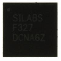
C8051F327-GM Silicon Laboratories Inc, C8051F327-GM Datasheet - Page 69

C8051F327-GM
Manufacturer Part Number
C8051F327-GM
Description
IC 8051 MCU FLASH 16K 28QFN
Manufacturer
Silicon Laboratories Inc
Series
C8051F32xr
Specifications of C8051F327-GM
Program Memory Type
FLASH
Program Memory Size
16KB (16K x 8)
Package / Case
28-QFN
Core Processor
8051
Core Size
8-Bit
Speed
25MHz
Connectivity
UART/USART, USB
Peripherals
POR
Number Of I /o
15
Ram Size
1.5K x 8
Voltage - Supply (vcc/vdd)
2.7 V ~ 3.6 V
Oscillator Type
Internal
Operating Temperature
-40°C ~ 85°C
Processor Series
C8051F3x
Core
8051
Data Bus Width
8 bit
Data Ram Size
1.5 KB
Interface Type
UART/USB
Maximum Clock Frequency
25 MHz
Number Of Programmable I/os
15
Number Of Timers
2
Operating Supply Voltage
2.7 V to 3.6 V
Maximum Operating Temperature
+ 85 C
Mounting Style
SMD/SMT
3rd Party Development Tools
PK51, CA51, A51, ULINK2
Development Tools By Supplier
C8051F326DK
Minimum Operating Temperature
- 40 C
Package
28QFN EP
Device Core
8051
Family Name
C8051F327
Maximum Speed
25 MHz
Lead Free Status / RoHS Status
Lead free / RoHS Compliant
For Use With
336-1481 - DAUGHTER CARD TOOLSTCK C8051F327770-1006 - ISP 4PORT FOR SILABS C8051F MCU
Eeprom Size
-
Data Converters
-
Lead Free Status / Rohs Status
Lead free / RoHS Compliant
Other names
336-1297-5
Available stocks
Company
Part Number
Manufacturer
Quantity
Price
Part Number:
C8051F327-GM
Manufacturer:
SILICON LABS/芯科
Quantity:
20 000
9.
The C8051F326/7 devices include 1280 bytes of on-chip XRAM. This XRAM space is split into user RAM
(addresses 0x0000–0x03FF) and USB0 FIFO space. The USB0 FIFO space is only accessible through the
USB FIFO registers.
9.1.
User XRAM can be accessed using the external move instruction (MOVX) and the data pointer (DPTR), or
using MOVX indirect addressing mode. If the MOVX instruction is used with an 8-bit address operand
(such as @R1), then the high byte of the 16-bit address is provided by the External Memory Interface Con-
trol Register (EMI0CN as shown in Figure 9.1). Note: the MOVX instruction is also used for writes to the
Flash memory. See Section “8. Flash Memory” on page 63 for details. The MOVX instruction accesses
XRAM by default.
For any of the addressing modes, the upper 6 bits of the 16-bit external data memory address word are
"don't cares". As a result, the 1024-byte RAM is mapped modulo style over the entire 64k external data
memory address range. For example, the XRAM byte at address 0x0000 is also at address 0x0400,
0x0800, 0x0C00, 0x1000, etc.
External RAM
Accessing User XRAM
0 x F F F F
0 x0 3 F F
0 x0 4 0 0
0 x0 0 0 0
Figure 9.1. External Ram Memory Map
0 x0 0 0 0 to 0 x 0 3 F F , w ra p p e d
S a m e 1 0 2 4 b y te s a s fro m
o n 1 K -b y te b o u n d a rie s
1 0 2 4 B y te s
X R A M
Rev. 1.1
A c ce ss e d o n ly th ro u g h U S B
F IF O re g iste rs (in a c ce ss ib le
u s in g th e M O V X in s tru ctio n)
A cc e s s e d w ith th e M O V X
in stru c tio n
U S B F IF O s
2 5 6 B y te s
C8051F326/7
69


