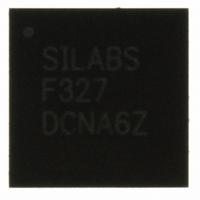
C8051F327-GM Silicon Laboratories Inc, C8051F327-GM Datasheet - Page 59

C8051F327-GM
Manufacturer Part Number
C8051F327-GM
Description
IC 8051 MCU FLASH 16K 28QFN
Manufacturer
Silicon Laboratories Inc
Series
C8051F32xr
Specifications of C8051F327-GM
Program Memory Type
FLASH
Program Memory Size
16KB (16K x 8)
Package / Case
28-QFN
Core Processor
8051
Core Size
8-Bit
Speed
25MHz
Connectivity
UART/USART, USB
Peripherals
POR
Number Of I /o
15
Ram Size
1.5K x 8
Voltage - Supply (vcc/vdd)
2.7 V ~ 3.6 V
Oscillator Type
Internal
Operating Temperature
-40°C ~ 85°C
Processor Series
C8051F3x
Core
8051
Data Bus Width
8 bit
Data Ram Size
1.5 KB
Interface Type
UART/USB
Maximum Clock Frequency
25 MHz
Number Of Programmable I/os
15
Number Of Timers
2
Operating Supply Voltage
2.7 V to 3.6 V
Maximum Operating Temperature
+ 85 C
Mounting Style
SMD/SMT
3rd Party Development Tools
PK51, CA51, A51, ULINK2
Development Tools By Supplier
C8051F326DK
Minimum Operating Temperature
- 40 C
Package
28QFN EP
Device Core
8051
Family Name
C8051F327
Maximum Speed
25 MHz
Lead Free Status / RoHS Status
Lead free / RoHS Compliant
For Use With
336-1481 - DAUGHTER CARD TOOLSTCK C8051F327770-1006 - ISP 4PORT FOR SILABS C8051F MCU
Eeprom Size
-
Data Converters
-
Lead Free Status / Rohs Status
Lead free / RoHS Compliant
Other names
336-1297-5
Available stocks
Company
Part Number
Manufacturer
Quantity
Price
Part Number:
C8051F327-GM
Manufacturer:
SILICON LABS/芯科
Quantity:
20 000
7.2.
When a power-down transition or power irregularity causes VDD to drop below V
monitor will drive the RST pin low and hold the CIP-51 in a reset state (see Figure 7.2). When VDD returns
to a level above V
memory contents are not altered by the power-fail reset, it is impossible to determine if VDD dropped
below the level required for data retention. If the PORSF flag reads ‘1’, the data may no longer be valid.
The VDD monitor is enabled after power-on resets; however its defined state (enabled/disabled) is not
altered by any other reset source. For example, if the VDD monitor is enabled and a software reset is per-
formed, the VDD monitor will still be enabled after the reset.
Important Note: The VDD monitor must be enabled before it is selected as a reset source. Selecting the
VDD monitor as a reset source before it is enabled and stabilized will cause a system reset. The procedure
for configuring the VDD monitor as a reset source is shown below:
See Figure 7.2 for VDD monitor timing. See Table 7.1 for complete electrical characteristics of the VDD
monitor.
Bit7:
Bit6:
Bits5–0: Reserved. Read = Variable. Write = don’t care.
VDMEN VDDSTAT Reserved Reserved Reserved Reserved Reserved Reserved
R/W
Bit7
Power-Fail Reset / VDD Monitor
Step 1. Enable the VDD monitor (VDM0CN.7 = ‘1’).
Step 2. Wait for the VDD monitor to stabilize (see Table 7.1 for the VDD Monitor turn-on time).
Step 3. Select the VDD monitor as a reset source (RSTSRC.1 = ‘1’).
VDMEN: VDD Monitor Enable.
This bit turns the VDD monitor circuit on/off. The VDD Monitor cannot generate system
resets until it is also selected as a reset source in register RSTSRC (Figure 7.2). The VDD
Monitor must be allowed to stabilize before it is selected as a reset source. Selecting the
VDD monitor as a reset source before it has stabilized may generate a system reset.
See Table 7.1 for the minimum VDD Monitor turn-on time. The VDD Monitor is enabled fol-
lowing all POR resets.
0: VDD Monitor Disabled.
1: VDD Monitor Enabled.
VDDSTAT: VDD Status.
This bit indicates the current power supply status (VDD Monitor output).
0: VDD is at or below the VDD monitor threshold.
1: VDD is above the VDD monitor threshold.
Bit6
RST
R
SFR Definition 7.1. VDM0CN: VDD Monitor Control
, the CIP-51 will be released from the reset state. Note that even though internal data
Bit5
R
Bit4
R
Rev. 1.1
Bit3
R
Bit2
R
Bit1
R
C8051F326/7
RST
Bit0
R
, the power supply
SFR Address:
Reset Value
Variable
0xFF
59


