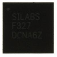
C8051F327-GM Silicon Laboratories Inc, C8051F327-GM Datasheet - Page 20

C8051F327-GM
Manufacturer Part Number
C8051F327-GM
Description
IC 8051 MCU FLASH 16K 28QFN
Manufacturer
Silicon Laboratories Inc
Series
C8051F32xr
Specifications of C8051F327-GM
Program Memory Type
FLASH
Program Memory Size
16KB (16K x 8)
Package / Case
28-QFN
Core Processor
8051
Core Size
8-Bit
Speed
25MHz
Connectivity
UART/USART, USB
Peripherals
POR
Number Of I /o
15
Ram Size
1.5K x 8
Voltage - Supply (vcc/vdd)
2.7 V ~ 3.6 V
Oscillator Type
Internal
Operating Temperature
-40°C ~ 85°C
Processor Series
C8051F3x
Core
8051
Data Bus Width
8 bit
Data Ram Size
1.5 KB
Interface Type
UART/USB
Maximum Clock Frequency
25 MHz
Number Of Programmable I/os
15
Number Of Timers
2
Operating Supply Voltage
2.7 V to 3.6 V
Maximum Operating Temperature
+ 85 C
Mounting Style
SMD/SMT
3rd Party Development Tools
PK51, CA51, A51, ULINK2
Development Tools By Supplier
C8051F326DK
Minimum Operating Temperature
- 40 C
Package
28QFN EP
Device Core
8051
Family Name
C8051F327
Maximum Speed
25 MHz
Lead Free Status / RoHS Status
Lead free / RoHS Compliant
For Use With
336-1481 - DAUGHTER CARD TOOLSTCK C8051F327770-1006 - ISP 4PORT FOR SILABS C8051F MCU
Eeprom Size
-
Data Converters
-
Lead Free Status / Rohs Status
Lead free / RoHS Compliant
Other names
336-1297-5
Available stocks
Company
Part Number
Manufacturer
Quantity
Price
Part Number:
C8051F327-GM
Manufacturer:
SILICON LABS/芯科
Quantity:
20 000
C8051F326/7
1.3.
The Universal Serial Bus Controller (USB0) is a USB 2.0 peripheral with integrated transceiver and end-
point FIFO RAM. The controller supports both full and low speed modes. A total of three endpoint pipes are
available: a bi-directional control endpoint (Endpoint0) and a data endpoint (Endpoint1) with one IN pipe
and one OUT pipe.
A 256 block of XRAM is used as dedicated USB FIFO space. This FIFO space is distributed between
Endpoint0 and Endpoint1. Endpoint0 is 64 bytes, and Endpoint1 has a 64 byte IN pipe and a 128 byte OUT
pipe.
USB0 can be operated as a Full or Low Speed function. The on-chip 4x Clock Multiplier and clock recovery
circuitry allow both Full and Low Speed options to be implemented with the on-chip precision oscillator as
the USB clock source. An external clock source can also be used with the 4x Clock Multiplier to generate
the USB clock.
The USB Transceiver is USB 2.0 compliant, and includes on-chip matching and pullup resistors. The pul-
lup resistors can be enabled/disabled in software, and will appear on the D+ or D– pin according to the
software-selected speed setting (full or low speed).
1.4.
C8051F326/7 devices include a voltage regulator (REG0). When enabled, the REG0 output appears on
the VDD pin and can be used to power external devices. REG0 can be enabled/disabled by software.
20
D+
D-
Universal Serial Bus Controller
Voltage Regulator
VDD
Transceiver
Figure 1.8. USB Controller Block Diagram
Transfer
Control
Data
Serial Interface Engine (SIE)
Rev. 1.1
IN
(256B RAM)
USB FIFOs
Endpoint0
Endpoint1
IN/OUT
OUT
Status, and
Registers
Interrupt
Control,
USB
CIP-51 Core


