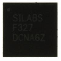
C8051F327-GM Silicon Laboratories Inc, C8051F327-GM Datasheet - Page 90

C8051F327-GM
Manufacturer Part Number
C8051F327-GM
Description
IC 8051 MCU FLASH 16K 28QFN
Manufacturer
Silicon Laboratories Inc
Series
C8051F32xr
Specifications of C8051F327-GM
Program Memory Type
FLASH
Program Memory Size
16KB (16K x 8)
Package / Case
28-QFN
Core Processor
8051
Core Size
8-Bit
Speed
25MHz
Connectivity
UART/USART, USB
Peripherals
POR
Number Of I /o
15
Ram Size
1.5K x 8
Voltage - Supply (vcc/vdd)
2.7 V ~ 3.6 V
Oscillator Type
Internal
Operating Temperature
-40°C ~ 85°C
Processor Series
C8051F3x
Core
8051
Data Bus Width
8 bit
Data Ram Size
1.5 KB
Interface Type
UART/USB
Maximum Clock Frequency
25 MHz
Number Of Programmable I/os
15
Number Of Timers
2
Operating Supply Voltage
2.7 V to 3.6 V
Maximum Operating Temperature
+ 85 C
Mounting Style
SMD/SMT
3rd Party Development Tools
PK51, CA51, A51, ULINK2
Development Tools By Supplier
C8051F326DK
Minimum Operating Temperature
- 40 C
Package
28QFN EP
Device Core
8051
Family Name
C8051F327
Maximum Speed
25 MHz
Lead Free Status / RoHS Status
Lead free / RoHS Compliant
For Use With
336-1481 - DAUGHTER CARD TOOLSTCK C8051F327770-1006 - ISP 4PORT FOR SILABS C8051F MCU
Eeprom Size
-
Data Converters
-
Lead Free Status / Rohs Status
Lead free / RoHS Compliant
Other names
336-1297-5
Available stocks
Company
Part Number
Manufacturer
Quantity
Price
Part Number:
C8051F327-GM
Manufacturer:
SILICON LABS/芯科
Quantity:
20 000
C8051F326/7
12.3. USB Register Access
The USB0 controller registers listed in Table 12.2 are accessed through two SFRs: USB0 Address
(USB0ADR) and USB0 Data (USB0DAT). The USB0ADR register selects which USB register is targeted
by reads/writes of the USB0DAT register. See Figure 12.2.
Endpoint control/status registers are accessed by first writing the USB register INDEX with the target end-
point number. Once the target endpoint number is written to the INDEX register, the control/status registers
associated with the target endpoint may be accessed. See the “Indexed Registers” section of Table 12.2
for a list of endpoint control/status registers.
Important Note: The USB clock must be active when accessing USB registers.
90
USB0ADR
USB0DAT
SFRs
8051
Figure 12.2. USB0 Register Access Scheme
Rev. 1.1
Registers
Registers
Common
Interrupt
Register
Access
Index
FIFO
USB Controller
Endpoint0 Control/
Endpoint1 Control/
Status Registers
Status Registers


