M68EVB908GB60E Freescale Semiconductor, M68EVB908GB60E Datasheet - Page 184
M68EVB908GB60E
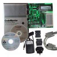
Manufacturer Part Number
M68EVB908GB60E
Description
BOARD EVAL FOR MC9S08GB60
Manufacturer
Freescale Semiconductor
Type
MCUr
Datasheet
1.M68EVB908GB60E.pdf
(290 pages)
Specifications of M68EVB908GB60E
Contents
Module and Misc Hardware
Processor To Be Evaluated
MC9S08GB
Data Bus Width
8 bit
Interface Type
RS-232
Silicon Manufacturer
Freescale
Core Architecture
HCS08
Core Sub-architecture
HCS08
Silicon Core Number
MC9S08
Silicon Family Name
S08GB
Kit Contents
GB60 Evaluation Kit
Rohs Compliant
Yes
For Use With/related Products
MC9S08GB60
Lead Free Status / RoHS Status
Lead free / RoHS Compliant


Serial Communications Interface (SCI) Module
RAF — Receiver Active Flag
11.10.6 SCI x Control Register 3 (SCIxC3)
R8 — Ninth Data Bit for Receiver
T8 — Ninth Data Bit for Transmitter
TXDIR — TxD1 Pin Direction in Single-Wire Mode
ORIE — Overrun Interrupt Enable
184
RAF is set when the SCI receiver detects the beginning of a valid start bit, and RAF is cleared
automatically when the receiver detects an idle line. This status flag can be used to check whether an
SCI character is being received before instructing the MCU to go to stop mode.
When the SCI is configured for 9-bit data (M = 1), R8 can be thought of as a ninth receive data bit to
the left of the MSB of the buffered data in the SCIxD register. When reading 9-bit data, both R8 and
SCIxD must be read to complete the automatic RDRF clearing sequence.
When the SCI is configured for 9-bit data (M = 1), T8 may be thought of as a ninth transmit data bit
to the left of the MSB of the data in the SCIxD register. When writing 9-bit data, the entire 9-bit value
is transferred to the SCI shift register after SCIxD is written so T8 should be written (if it needs to
change from its previous value) before SCIxD is written. If T8 does not need to change in the new
value (such as when it is used to generate mark or space parity), it need not be written each time SCIxD
is written.
When the SCI is configured for single-wire half-duplex operation (LOOPS = RSRC = 1), this bit
determines the direction of data at the TxD1 pin.
This bit enables the overrun flag (OR) to generate hardware interrupt requests.
1 = SCI receiver active (RxD1 input not idle).
0 = SCI receiver idle waiting for a start bit.
1 = TxD1 pin is an output in single-wire mode.
0 = TxD1 pin is an input in single-wire mode.
1 = Hardware interrupt requested when OR = 1.
0 = OR interrupts disabled (use polling).
Reset:
Read:
Write:
Bit 7
Figure 11-11. SCI x Control Register 3 (SCIxC3)
R8
0
= Unimplemented or Reserved
MC9S08GB/GT Data Sheet, Rev. 2.3
T8
6
0
TXDIR
5
0
4
0
0
ORIE
3
0
NEIE
2
0
FEIE
Freescale Semiconductor
1
0
PEIE
Bit 0
0
Related parts for M68EVB908GB60E
Image
Part Number
Description
Manufacturer
Datasheet
Request
R

Part Number:
Description:
Manufacturer:
Freescale Semiconductor, Inc
Datasheet:
Part Number:
Description:
Manufacturer:
Freescale Semiconductor, Inc
Datasheet:
Part Number:
Description:
Manufacturer:
Freescale Semiconductor, Inc
Datasheet:
Part Number:
Description:
Manufacturer:
Freescale Semiconductor, Inc
Datasheet:
Part Number:
Description:
Manufacturer:
Freescale Semiconductor, Inc
Datasheet:
Part Number:
Description:
Manufacturer:
Freescale Semiconductor, Inc
Datasheet:
Part Number:
Description:
Manufacturer:
Freescale Semiconductor, Inc
Datasheet:
Part Number:
Description:
Manufacturer:
Freescale Semiconductor, Inc
Datasheet:
Part Number:
Description:
Manufacturer:
Freescale Semiconductor, Inc
Datasheet:
Part Number:
Description:
Manufacturer:
Freescale Semiconductor, Inc
Datasheet:
Part Number:
Description:
Manufacturer:
Freescale Semiconductor, Inc
Datasheet:
Part Number:
Description:
Manufacturer:
Freescale Semiconductor, Inc
Datasheet:
Part Number:
Description:
Manufacturer:
Freescale Semiconductor, Inc
Datasheet:
Part Number:
Description:
Manufacturer:
Freescale Semiconductor, Inc
Datasheet:
Part Number:
Description:
Manufacturer:
Freescale Semiconductor, Inc
Datasheet: