M68EVB908GB60E Freescale Semiconductor, M68EVB908GB60E Datasheet - Page 172
M68EVB908GB60E
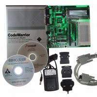
Manufacturer Part Number
M68EVB908GB60E
Description
BOARD EVAL FOR MC9S08GB60
Manufacturer
Freescale Semiconductor
Type
MCUr
Datasheet
1.M68EVB908GB60E.pdf
(290 pages)
Specifications of M68EVB908GB60E
Contents
Module and Misc Hardware
Processor To Be Evaluated
MC9S08GB
Data Bus Width
8 bit
Interface Type
RS-232
Silicon Manufacturer
Freescale
Core Architecture
HCS08
Core Sub-architecture
HCS08
Silicon Core Number
MC9S08
Silicon Family Name
S08GB
Kit Contents
GB60 Evaluation Kit
Rohs Compliant
Yes
For Use With/related Products
MC9S08GB60
Lead Free Status / RoHS Status
Lead free / RoHS Compliant


Serial Communications Interface (SCI) Module
If no new character is waiting in the transmit data buffer after a stop bit is shifted out the TxD1 pin, the
transmitter sets the transmit complete flag and enters an idle mode, with TxD1 high, waiting for more
characters to transmit.
Writing 0 to TE does not immediately release the pin to be a general-purpose I/O pin. Any transmit activity
that is in progress must first be completed. This includes data characters in progress, queued idle
characters, and queued break characters.
11.5.2
The SBK control bit in SCIxC2 is used to send break characters that were originally used to gain the
attention of old teletype receivers. Break characters are a full character time of logic 0 (including a 0 where
the stop bit would be normally). Normally, a program would wait for TDRE to become set to indicate the
last character of a message has moved to the transmit shifter, then write 1 and then write 0 to the SBK bit.
This action queues a break character to be sent as soon as the shifter is available. If SBK is still 1 when the
queued break moves into the shifter (synchronized to the baud rate clock), an additional break character is
queued. If the receiving device is another Freescale Semiconductor SCI, the break characters will be
received as 0s in all eight (or nine) data bits and a framing error (FE = 1).
When idle-line wakeup is used, a full character time of idle (logic 1) is needed between messages to wake
up any sleeping receivers. Normally, a program would wait for TDRE to become set to indicate the last
character of a message has moved to the transmit shifter, then write 0 and then write 1 to the TE bit. This
action queues an idle character to be sent as soon as the shifter is available. As long as the character in the
shifter does not finish while TE = 0, the SCI transmitter never actually releases control of the TxD1 pin. If
there is a possibility of the shifter finishing while TE = 0, set the general-purpose I/O controls so the pin
that is shared with TxD1 is an output driving a logic 1. This ensures that the TxD1 line will look like a
normal idle line even if the SCI loses control of the port pin between writing 0 and then 1 to TE.
11.6
In this section, the receiver block diagram
functional description. Next, the data sampling technique used to reconstruct receiver data is described in
more detail. Finally, two variations of the receiver wakeup function are explained.
11.6.1
Figure 11-4
172
Receiver Functional Description
Send Break and Queued Idle
Receiver Block Diagram
shows the receiver portion of the SCI.
MC9S08GB/GT Data Sheet, Rev. 2.3
(Figure
11-4) is used as a guide for the overall receiver
Freescale Semiconductor
Related parts for M68EVB908GB60E
Image
Part Number
Description
Manufacturer
Datasheet
Request
R

Part Number:
Description:
Manufacturer:
Freescale Semiconductor, Inc
Datasheet:
Part Number:
Description:
Manufacturer:
Freescale Semiconductor, Inc
Datasheet:
Part Number:
Description:
Manufacturer:
Freescale Semiconductor, Inc
Datasheet:
Part Number:
Description:
Manufacturer:
Freescale Semiconductor, Inc
Datasheet:
Part Number:
Description:
Manufacturer:
Freescale Semiconductor, Inc
Datasheet:
Part Number:
Description:
Manufacturer:
Freescale Semiconductor, Inc
Datasheet:
Part Number:
Description:
Manufacturer:
Freescale Semiconductor, Inc
Datasheet:
Part Number:
Description:
Manufacturer:
Freescale Semiconductor, Inc
Datasheet:
Part Number:
Description:
Manufacturer:
Freescale Semiconductor, Inc
Datasheet:
Part Number:
Description:
Manufacturer:
Freescale Semiconductor, Inc
Datasheet:
Part Number:
Description:
Manufacturer:
Freescale Semiconductor, Inc
Datasheet:
Part Number:
Description:
Manufacturer:
Freescale Semiconductor, Inc
Datasheet:
Part Number:
Description:
Manufacturer:
Freescale Semiconductor, Inc
Datasheet:
Part Number:
Description:
Manufacturer:
Freescale Semiconductor, Inc
Datasheet:
Part Number:
Description:
Manufacturer:
Freescale Semiconductor, Inc
Datasheet: