ADIS16355/PCBZ Analog Devices Inc, ADIS16355/PCBZ Datasheet - Page 18
ADIS16355/PCBZ
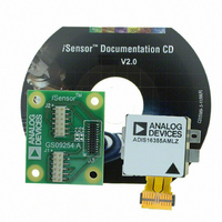
Manufacturer Part Number
ADIS16355/PCBZ
Description
BOARD EVAL FOR ADIS16355
Manufacturer
Analog Devices Inc
Series
iMEMS®, iSensor™r
Datasheets
1.ADIS16350PCBZ.pdf
(24 pages)
2.ADIS16350PCBZ.pdf
(2 pages)
3.ADIS16355PCBZ.pdf
(2 pages)
Specifications of ADIS16355/PCBZ
Sensor Type
Accelerometer, Gyroscope, 3 Axis
Sensing Range
±10g, ±75°/sec, ±150°/sec, ±300°/sec
Interface
SPI Serial
Sensitivity
2.522mg/LSB, 0.018°/sec/LSB
Voltage - Supply
4.75 V ~ 5.25 V
Embedded
No
Utilized Ic / Part
ADIS16355
For Use With
ADISUSBZ - KIT EVAL ADIS W/SOFTWARE USB
Lead Free Status / RoHS Status
Lead free / RoHS Compliant


ADIS16350/ADIS16355
Dynamic Range
There are three dynamic range settings: ±75°/s, ±150°/s, and
±300°/s. The lower dynamic range settings (75, 150) limit the
minimum filter tap sizes to maintain the resolution as the measure-
ment range decreases. The recommended order for programming
the SENS/AVG register is upper byte (sensitivity), followed by
lower byte (filtering). The contents of the SENS/AVG register
are nonvolatile.
Table 20. SENS/AVG Register Definition
Address
0x39, 0x38
Table 21. SENS/AVG Bit Descriptions
Bits
[15:11]
[10:8]
[7:3]
[2:0]
Auxiliary DAC
The auxiliary DAC provides a 12-bit level adjustment function.
The AUX_DAC register controls the operation of this feature.
It offers a rail-to-rail buffered output that has a range of 0 V
to 2.5 V. The DAC can drive its output to within 5 mV of the
ground reference when it is not sinking current. As the output
approaches ground, the linearity begins to degrade (100 LSB
beginning point). As the sink current increases, the nonlinear
range increases. The DAC output latch function, contained in
the COMMAND register, provides continuous operation while
writing each byte of this register. The contents of this register
are volatile, which means that the desired output level must be
set after every reset and power cycle event.
–100
–120
–140
–20
–40
–60
–80
0.001
0
Figure 27. Bartlett Window FIR Frequency Response
Default
0x0402
Value
100
010
001
N = 2
N = 4
N = 16
N = 64
0.01
Description
Not used
Measurement range (sensitivity)
selection
300°/s (default condition)
150°/s, filter taps ≥ 4 (Bits [2:0] ≥ 0x02)
75°/s, filter taps ≥ 16 (Bits [2:0] ≥ 0x04)
Not used
Filter tap setting, number of taps,
N = 2
Format
N/A
FREQUENCY (
M
; for example, 011, N = 2
f
/
f
S
)
0.1
Access
R/W
3
= 8 taps
1
Rev. B | Page 18 of 24
Table 22. AUX_DAC Register Definition
Address
0x31, 0x30
Table 23. AUX_DAC Bit Descriptions
Bits
[15:12]
[11:0]
Updating the DAC output voltage requires four steps.
1.
2.
3.
4.
General-Purpose Input/Output
Two general-purpose pins enable digital input/output control
using the SPI. The GPIO_CTRL control register establishes the
configuration of these pins and handles the SPI-to-pin controls.
Each pin provides the flexibility of both input (read) and output
(write) operations.
For example, writing 0x0202 to this register establishes Line 2 as
an output and sets its level as a 1. Writing 0x0000 to this register
establishes both lines as inputs, and their status can be read through
Bit 8 and Bit 9 of this register.
The digital input/output lines are also available for data-ready and
alarm/error indications. In the event of conflict, the following
priority structure governs the digital input/output configuration:
1.
2.
3.
Table 24. GPIO_CTRL Register Definition
Address
0x33, 0x32
Table 25. GPIO_CTRL Bit Descriptions
Bits
[15:10]
[9]
[8]
[7:2]
[1]
[0]
The contents of the GPIO_CTRL register are volatile.
Determine the binary number associated with the desired
output level.
Write the lower eight bits of this binary number to the
lower address of the AUX_DAC register.
Write the upper eight bits of this binary number to the
upper address of the AUX_DAC register.
Execute the DAC latch global command by writing 0x04 to
Address 0x3E (see Table 15).
MSC_CTRL (Data-ready indicator)
ALM_CTRL (Alarm indicator)
GPIO_CTRL (General-purpose)
Description
Not used
General-purpose input/output Line 2 data level
General-purpose input/output Line 1 data level
Not used
General-purpose input/output Line 2, data direction
control
General-purpose input/output Line 1, data direction
control
Description
Not used
Data bits; 0x0000 – 0 V output, 0x0FFF – 2.5 V output
1 = high, 0 = low
1 = high, 0 = low
1 = output, 0 = input
1 = output, 0 = input
Default
0x0000
Default
0x0000
Format
N/A
Format
Binary
Access
R/W
Access
R/W
Related parts for ADIS16355/PCBZ
Image
Part Number
Description
Manufacturer
Datasheet
Request
R

Part Number:
Description:
PC EVALUATION SYSTEM
Manufacturer:
Analog Devices Inc
Datasheet:

Part Number:
Description:
±1.7g Dual-Axis IMEMS Accelerometer Evaluation Board
Manufacturer:
Analog Devices Inc
Datasheet:
Part Number:
Description:
Inertial Sensor Evaluation System
Manufacturer:
Analog Devices Inc
Datasheet:
Part Number:
Description:
Manufacturer:
Analog Devices Inc
Datasheet:
Part Number:
Description:
Manufacturer:
Analog Devices Inc
Datasheet:
Part Number:
Description:
Manufacturer:
Analog Devices Inc
Datasheet:
Part Number:
Description:
Manufacturer:
Analog Devices Inc
Datasheet:
Part Number:
Description:
Manufacturer:
Analog Devices Inc
Datasheet:
Part Number:
Description:
Manufacturer:
Analog Devices Inc
Datasheet:
Part Number:
Description:
Manufacturer:
Analog Devices Inc
Datasheet:
Part Number:
Description:
Manufacturer:
Analog Devices Inc
Datasheet:
Part Number:
Description:
Manufacturer:
Analog Devices Inc
Datasheet:
Part Number:
Description:
Manufacturer:
Analog Devices Inc
Datasheet: