ADIS16355/PCBZ Analog Devices Inc, ADIS16355/PCBZ Datasheet - Page 13
ADIS16355/PCBZ
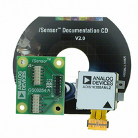
Manufacturer Part Number
ADIS16355/PCBZ
Description
BOARD EVAL FOR ADIS16355
Manufacturer
Analog Devices Inc
Series
iMEMS®, iSensor™r
Datasheets
1.ADIS16350PCBZ.pdf
(24 pages)
2.ADIS16350PCBZ.pdf
(2 pages)
3.ADIS16355PCBZ.pdf
(2 pages)
Specifications of ADIS16355/PCBZ
Sensor Type
Accelerometer, Gyroscope, 3 Axis
Sensing Range
±10g, ±75°/sec, ±150°/sec, ±300°/sec
Interface
SPI Serial
Sensitivity
2.522mg/LSB, 0.018°/sec/LSB
Voltage - Supply
4.75 V ~ 5.25 V
Embedded
No
Utilized Ic / Part
ADIS16355
For Use With
ADISUSBZ - KIT EVAL ADIS W/SOFTWARE USB
Lead Free Status / RoHS Status
Lead free / RoHS Compliant


BASIC OPERATION
The ADIS16350/ADIS16355 are designed for simple integration
into system designs, requiring only a 5 V power supply and a
4-wire, industry-standard serial peripheral interface (SPI). All
outputs and user-programmable functions are handled by a
simple register structure. Each register is 16 bits in length and
has its own unique bit map. The 16 bits in each register consist
of an upper byte (D8 to D15) and a lower byte (D0 to D7), each
with its own 6-bit address.
SERIAL PERIPHERAL INTERFACE (SPI)
The serial peripheral interface (SPI) port includes four signals:
chip select ( CS ), serial clock (SCLK), data input (DIN), and data
output (DOUT). The CS line enables the SPI port and frames
each SPI event. When this signal is high, the DOUT line is in a
high impedance state and the signals on DIN and SCLK have no
impact on operation. A complete data frame contains 16 clock
cycles. Because the SPI port operates in full-duplex mode, it
supports simultaneous, 16-bit receive (DIN) and transmit (DOUT)
functions during the same data frame. This enables the user to
configure the next read cycle, while, at the same time, receiving
the data associated with the previous configuration.
Refer to Table 2, Figure 2, and Figure 3 for detailed information
regarding timing and operation of the SPI port.
DOUT
SCLK
W/R BIT
SCLK
DIN
CS
DIN
CS
WRITE = 1
READ = 0
W/R
BASED ON PREVIOUS COMMAND
ZERO
ADDRESS
A5
DATA FRAME
REGISTER ADDRESS
A4
Figure 26. SPI Sequence for Read Commands
A3
A2
Figure 25. DIN Bit Sequence
DON’T CARE
Rev. B | Page 13 of 24
A1
DATA FRAME
A0
DC7
Writing to Registers
Figure 25 displays a typical data frame for writing a command
to a control register. In this case, the first bit of the DIN sequence
is a 1, followed by a 0, the 6-bit address of the target register,
and the 8-bit data command. Because each write command
covers a single byte of data, two data frames are required when
writing the entire 16-bit space of a register. Note that 16 SCLK
cycles are required for a successful write operation.
Reading from Registers
Reading the contents of a register requires a modification to the
sequence illustrated in Figure 25. In this case, the first two bits
in the DIN sequence are 0, followed by the address of the register.
Each register has two addresses (an upper address and a lower
address), but either one can be used to access the entire 16 bits of
data. The final eight bits of the DIN sequence are irrelevant and can
be counted as don’t cares during a read command. During the next
data frame, the DOUT sequence contains the 16-bit data of the
register, as shown in Figure 26. Although a single read command
requires two separate data frames, the full-duplex mode mini-
mizes this overhead, requiring only one extra data frame when
continuously sampling.
DON’T CARE FOR READ COMMANDS
DC6
DATA FOR WRITE COMMANDS
DC5 DC4
16-BIT REGISTER CONTENTS
DATA FRAME
NEXT COMMAND
DC3 DC2 DC1
ADIS16350/ADIS16355
DC0
Related parts for ADIS16355/PCBZ
Image
Part Number
Description
Manufacturer
Datasheet
Request
R

Part Number:
Description:
PC EVALUATION SYSTEM
Manufacturer:
Analog Devices Inc
Datasheet:

Part Number:
Description:
±1.7g Dual-Axis IMEMS Accelerometer Evaluation Board
Manufacturer:
Analog Devices Inc
Datasheet:
Part Number:
Description:
Inertial Sensor Evaluation System
Manufacturer:
Analog Devices Inc
Datasheet:
Part Number:
Description:
Manufacturer:
Analog Devices Inc
Datasheet:
Part Number:
Description:
Manufacturer:
Analog Devices Inc
Datasheet:
Part Number:
Description:
Manufacturer:
Analog Devices Inc
Datasheet:
Part Number:
Description:
Manufacturer:
Analog Devices Inc
Datasheet:
Part Number:
Description:
Manufacturer:
Analog Devices Inc
Datasheet:
Part Number:
Description:
Manufacturer:
Analog Devices Inc
Datasheet:
Part Number:
Description:
Manufacturer:
Analog Devices Inc
Datasheet:
Part Number:
Description:
Manufacturer:
Analog Devices Inc
Datasheet:
Part Number:
Description:
Manufacturer:
Analog Devices Inc
Datasheet:
Part Number:
Description:
Manufacturer:
Analog Devices Inc
Datasheet: