ADIS16355/PCBZ Analog Devices Inc, ADIS16355/PCBZ Datasheet - Page 17
ADIS16355/PCBZ
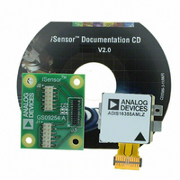
Manufacturer Part Number
ADIS16355/PCBZ
Description
BOARD EVAL FOR ADIS16355
Manufacturer
Analog Devices Inc
Series
iMEMS®, iSensor™r
Datasheets
1.ADIS16350PCBZ.pdf
(24 pages)
2.ADIS16350PCBZ.pdf
(2 pages)
3.ADIS16355PCBZ.pdf
(2 pages)
Specifications of ADIS16355/PCBZ
Sensor Type
Accelerometer, Gyroscope, 3 Axis
Sensing Range
±10g, ±75°/sec, ±150°/sec, ±300°/sec
Interface
SPI Serial
Sensitivity
2.522mg/LSB, 0.018°/sec/LSB
Voltage - Supply
4.75 V ~ 5.25 V
Embedded
No
Utilized Ic / Part
ADIS16355
For Use With
ADISUSBZ - KIT EVAL ADIS W/SOFTWARE USB
Lead Free Status / RoHS Status
Lead free / RoHS Compliant


Table 14. COMMAND Register Definition
Address
0x3F, 0x3E
Table 15. COMMAND Bit Descriptions
Bits
[15:8]
[7]
[6:5]
[4]
[3]
[2]
[1]
[0]
OPERATIONAL CONTROL
Internal Sample Rate
The internal sample rate defines how often data output variables
are updated, independent of the rate at which they are read out on
the SPI port. The SMPL_PRD register controls the internal sample
rate and has two parts: a time base and a multiplier. The sample
period can be calculated using the following equation:
where:
T
T
N
The default value is the minimum register setting, 0x01, which
corresponds to the maximum sample rate of 819.2 samples per
second. The contents of this register are nonvolatile.
Table 16. SMPL_PRD Register Definition
Address
0x37, 0x36
Table 17. SMPL_PRD Bit Descriptions
Bits
[15:8]
[7]
[6:0]
An example calculation of the sample period for the device is
The sample rate setting has a direct impact on the SPI data rate
capability. For SMPL_PRD settings ≤ 0x09 (fast mode), the SPI
SCLK can run at a rate up to 2.0 MHz. For SMPL_PRD settings >
0x09 (normal mode), the SPI SCLK can run at a rate up to 300 kHz.
S
B
S
is the sample period.
is the time base.
is the multiplier.
T
If SMPL_PRD = 0x0007, Bits [7:0] = 00000111
Bit 7 = 0, so T
Bits [6:0] = 0000111 = 7 = N
T
f
S
S
S
= 1∕T
= T
= T
Description
Not used
Software reset command
Not used
Precision autonull command
Flash update command
Auxiliary DAC data latch
Factory calibration restore command
Autonull command
Description
Not used
Time base, 0 = 0.61035 ms, 1 = 18.921 ms
Multiplier (add 1 before multiplying by the time base)
B
B
S
× (N
× (N
= 204.8 SPS
Default
N/A
Default
0x0001
S
S
+ 1)
+ 1) = 0.61035 ms × (7 + 1) = 4.8828 ms
B
= 0.61035 ms
S
Format
N/A
Format
N/A
Access
Write only
Access
R/W
Rev. B | Page 17 of 24
The sample rate setting also affects the power dissipation.
The normal mode power (SMPL_PRD > 0x09) dissipation is
approximately 67% less than the fast mode (SMPL_PRD ≤ 0x09)
power dissipation. The two different modes of operation offer a
system-level trade-off between performance (sample rate, serial
transfer rate) and power dissipation.
Power Management
In addition to offering two different performance modes for power
optimization, the SLP_CNT register provides a programmable
shutdown period. Writing the appropriate sleep time to the lower
byte of the SLP_CNT register shuts the device down for the
specified time. The following example illustrates this relationship:
At the completion of the programmed duration, normal operation
resumes. If measurements are required before sleep period
completion or if it is necessary to end the indefinite shutdown,
the device can be awakened by pulling the CS line down to a 0
state, then returning it to a 1 state. Otherwise, the CS line must
be kept in a 1 (high) state to maintain sleep mode.
When writing a sleep time to the SLP_CNT register, the time
between the 16
than 10 μs in fast mode and less than 80 μs in normal mode.
Table 18. SLP_CNT Register Definition
Address
0x3B, 0x3A
1
Table 19. SLP_CNT Bit Descriptions
Bits
[15:8]
[7:0]
Digital Filtering
The signal conditioning circuit of each sensor has an analog
bandwidth of approximately 350 Hz. A programmable-length
Bartlett Window FIR filter provides opportunity for additional
noise reduction on all of the output data registers. The
SENS/AVG register controls the number of taps in power-of-two
step sizes, from zero to six.
Filter setup requires one simple step: write the appropriate M
factor to the assigned bits in the SENS/AVG register. The bit
assignments are listed in Table 21. The frequency response
relationship for this filter is:
Scale is the weight of each LSB in the lower byte of this register.
Bits [7:0] = 00000110 = 6 codes = 3 seconds
H
Description
Not used
Data bits
B
(
Scale
0.5 sec
f
th
)
=
SCLK edge and the CS rising edge must be less
H
1
2
A
(
f
Default
0x0000
)
H
ADIS16350/ADIS16355
A
(
f
)
=
Format
Binary
sin
N
×
(
π
sin
×
(
N
π
Access
R/W
× ×
×
f
f
×
t
t
s
s
)
)
Related parts for ADIS16355/PCBZ
Image
Part Number
Description
Manufacturer
Datasheet
Request
R

Part Number:
Description:
PC EVALUATION SYSTEM
Manufacturer:
Analog Devices Inc
Datasheet:

Part Number:
Description:
±1.7g Dual-Axis IMEMS Accelerometer Evaluation Board
Manufacturer:
Analog Devices Inc
Datasheet:
Part Number:
Description:
Inertial Sensor Evaluation System
Manufacturer:
Analog Devices Inc
Datasheet:
Part Number:
Description:
Manufacturer:
Analog Devices Inc
Datasheet:
Part Number:
Description:
Manufacturer:
Analog Devices Inc
Datasheet:
Part Number:
Description:
Manufacturer:
Analog Devices Inc
Datasheet:
Part Number:
Description:
Manufacturer:
Analog Devices Inc
Datasheet:
Part Number:
Description:
Manufacturer:
Analog Devices Inc
Datasheet:
Part Number:
Description:
Manufacturer:
Analog Devices Inc
Datasheet:
Part Number:
Description:
Manufacturer:
Analog Devices Inc
Datasheet:
Part Number:
Description:
Manufacturer:
Analog Devices Inc
Datasheet:
Part Number:
Description:
Manufacturer:
Analog Devices Inc
Datasheet:
Part Number:
Description:
Manufacturer:
Analog Devices Inc
Datasheet: