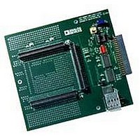
ADZS-21262-1-EZEXT Analog Devices Inc, ADZS-21262-1-EZEXT Datasheet - Page 15

ADZS-21262-1-EZEXT
Manufacturer Part Number
ADZS-21262-1-EZEXT
Description
BOARD DAUGHTER FOR ADSP-21262
Manufacturer
Analog Devices Inc
Datasheet
1.ADSP-21363KSWZ-1AA.pdf
(56 pages)
Specifications of ADZS-21262-1-EZEXT
Accessory Type
DSP
Silicon Manufacturer
Analog Devices
Core Architecture
SHARC
Features
Expansion Interface, High Speed Converter (HSC) Interface
Kit Contents
Board Docs
Silicon Family Name
SHARC
Silicon Core Number
ADSP-21262
Rohs Compliant
Yes
Lead Free Status / RoHS Status
Lead free / RoHS Compliant
For Use With/related Products
ADSP-21262
Lead Free Status / RoHS Status
Lead free / RoHS Compliant, Lead free / RoHS Compliant
PACKAGE INFORMATION
The information presented in
the package branding for the ADSP-2136x processor. For a
complete listing of product availability, see
Page
Table 7. Package Brand Information
ESD CAUTION
MAXIMUM POWER DISSIPATION
See Estimating Power for the ADSP-21362 SHARC Processors
(EE-277) for detailed thermal and power information regarding
maximum power dissipation. For information on package ther-
mal specifications, see
ABSOLUTE MAXIMUM RATINGS
Stresses greater than those listed in
nent damage to the device. These are stress ratings only;
functional operation of the device at these or any other condi-
tions greater than those indicated in the operational sections of
this specification is not implied. Exposure to absolute maximum
rating conditions for extended periods may affect device
reliability.
Brand Key
t
pp
Z
cc
vvvvvv.x
n.n
#
yyww
54.
ESD (electrostatic discharge) sensitive device.
Charged devices and circuit boards can discharge
without detection. Although this product features
patented or proprietary protection circuitry, damage
may occur on devices subjected to high energy ESD.
Therefore, proper ESD precautions should be taken to
avoid performance degradation or loss of functionality.
Figure 4. Typical Package Brand
Thermal Characteristics on Page
#yyww country_of_origin
ADSP-21362/ADSP-21363/ADSP-21364/ADSP-21365/ADSP-21366
ADSP-2136x
vvvvvv.x n.n
Field Description
Temperature Range
Package Type
RoHS Compliant Designation
See Ordering Guide
Assembly Lot Code
Silicon Revision
RoHS Compliant Designation
Date Code
Figure 4
tppZ-cc
Table 8
provides details about
Ordering Guide on
may cause perma-
Rev. G | Page 15 of 56 | March 2011
45.
Table 8. Absolute Maximum Ratings
TIMING SPECIFICATIONS
Use the exact timing information given. Do not attempt to
derive parameters from the addition or subtraction of others.
While addition or subtraction would yield meaningful results
for an individual device, the values given in this data sheet
reflect statistical variations and worst cases. Consequently, it is
not meaningful to add parameters to derive longer times. For
voltage reference levels, see
Conditions
Switching Characteristics specify how the processor changes its
signals. Circuitry external to the processor must be designed for
compatibility with these signal characteristics. Switching char-
acteristics describe what the processor will do in a given
circumstance. Use switching characteristics to ensure that any
timing requirement of a device connected to the processor (such
as memory) is satisfied.
Timing Requirements apply to signals that are controlled by cir-
cuitry external to the processor, such as the data input for a read
operation. Timing requirements guarantee that the processor
operates correctly with other devices.
Core Clock Requirements
The processor’s internal clock (a multiple of CLKIN) provides
the clock signal for timing internal memory, processor core, and
serial ports. During reset, program the ratio between the proces-
sor’s internal clock frequency and external (CLKIN) clock
frequency with the CLK_CFG1–0 pins.
The processor’s internal clock switches at higher frequencies
than the system input clock (CLKIN). To generate the internal
clock, the processor uses an internal phase-locked loop (PLL,
see
between the system clock (CLKIN) signal and the processor’s
internal clock.
Voltage Controlled Oscillator
In application designs, the PLL multiplier value should be
selected in such a way that the VCO frequency never exceeds
f
Parameter
Internal (Core) Supply Voltage (V
Analog (PLL) Supply Voltage (A
External (I/O) Supply Voltage (V
Input Voltage
Output Voltage Swing
Load Capacitance
Storage Temperature Range
Junction Temperature While Biased
VCO
• The product of CLKIN and PLLM must never exceed 1/2
Figure
f
(INDIV = 0).
specified in
VCO
(max) in
5). This PLL-based clocking minimizes the skew
.
Table
Table 11
11.
Figure 39 on Page 44
if the input divider is not enabled
VDD
DDEXT
DDINT
)
)
)
Rating
–0.3 V to +1.5 V
–0.3 V to +1.5 V
–0.3 V to +4.6 V
–0.5 V to +3.8 V
–0.5 V to V
200 pF
–65°C to +150°C
125°C
under
DDEXT
Test
+ 0.5 V


