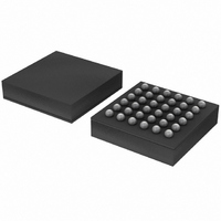
SC16C852SVIET,115 NXP Semiconductors, SC16C852SVIET,115 Datasheet - Page 5

SC16C852SVIET,115
Manufacturer Part Number
SC16C852SVIET,115
Description
IC UART DL 1.8V W/FIFO 36-TFBGA
Manufacturer
NXP Semiconductors
Datasheet
1.SC16C852SVIET151.pdf
(48 pages)
Specifications of SC16C852SVIET,115
Features
Programmable
Number Of Channels
2, DUART
Fifo's
128 Byte
Protocol
RS485
Voltage - Supply
1.8V
With Auto Flow Control
Yes
With Irda Encoder/decoder
Yes
With False Start Bit Detection
Yes
With Modem Control
Yes
With Cmos
Yes
Mounting Type
Surface Mount
Package / Case
36-TFBGA
Lead Free Status / RoHS Status
Lead free / RoHS Compliant
Other names
935286451115
SC16C852SVIET-G
SC16C852SVIET-G
SC16C852SVIET-G
SC16C852SVIET-G
Available stocks
Company
Part Number
Manufacturer
Quantity
Price
Company:
Part Number:
SC16C852SVIET,115
Manufacturer:
NXP Semiconductors
Quantity:
10 000
NXP Semiconductors
SC16C852SV_1
Product data sheet
Table 2.
Symbol
CS
CTSA
CTSB
DSRA
DSRB
DTRA
DTRB
INTA
INTB
IOR
IOW
LLA
LOWPWR F1
Pin description
Pin
E2
A6
F6
A5
E4
C5
B6
D5
D6
F4
E3
E6
Dual UART with 128-byte FIFOs, IrDA, and XScale VLIO bus interface
Type
I
I
I
O
O
O
I
I
I
I
Rev. 01 — 23 September 2008
…continued
Description
Chip Select (active LOW). This pin enables the data transfers
between the host and the SC16C852SV for the addressed channel.
Individual channel selection is done with address A6. When A6 is 0
channel A is selected, and when A6 is 1 channel B is selected.
Clear to Send (active LOW). These inputs are associated with
individual UART channels, A through B. A logic 0 on the CTS pin
indicates the modem or data set is ready to accept transmit data from
the SC16C852SV. Status can be tested by reading MSR[4].
Data Set Ready (active LOW). These inputs are associated with
individual UART channels, A through B. A logic 0 on this pin indicates
the modem or data set is powered-on and is ready for data exchange
with the UART. Status can be tested by reading MSR[5].
Data Terminal Ready (active LOW). These outputs are associated
with individual UART channels, A through B. A logic 0 on this pin
indicates that the SC16C852SV is powered-on and ready. This pin
can be controlled via the Modem Control Register. Writing a logic 1 to
MCR[0] will set the DTR output to logic 0, enabling the modem. This
pin will be a logic 1 after writing a logic 0 to MCR[0], or after a reset.
Channel A interrupt output. The output state is defined by the user
through the software setting of MCR[3]. INTA is set to the active
mode when MCR[3] is set to a logic 1. INTA is set to the 3-state mode
when MCR[3] is set to a logic 0. See
Channel B interrupt output. The output state is defined by the user
through the software setting of MCR[3]. INTB is set to the active
mode when MCR[3] is set to a logic 1. INTB is set to the 3-state
mode when MCR[3] is set to a logic 0. See
Read strobe (active LOW). A HIGH to LOW transition on this signal
starts the read cycle. The SC16C852SV reads a byte from the
internal register and puts the byte on the data bus for the host to
retrieve.
Write strobe (active LOW). A HIGH to LOW transition on this signal
starts the write cycle, and a LOW to HIGH transition transfers the
data on the data bus to the internal register.
Latch Lower Address (active LOW). A logic LOW on this pin puts
the VLIO interface in the address phase of the transaction, where the
lower 8 bits of the VLIO (specifying the UART register and the
channel address) are loaded into the address latch of the device
through the AD7 to AD0 bus. A logic HIGH puts the VLIO interface in
the data phase where data can are transferred between the host and
the UART.
Low Power. When asserted (active HIGH), the device immediately
goes into low power mode. The oscillator is shut-off and some host
interface pins are isolated from the host’s bus to reduce power
consumption. The device only returns to normal mode when the
LOWPWR pin is de-asserted. On the negative edge of a de-asserting
LOWPWR signal, the device is automatically reset and all registers
return to their default reset states. This pin has an internal pull-down
resistor, therefore, it can be left unconnected.
Table
SC16C852SV
19.
Table
© NXP B.V. 2008. All rights reserved.
19.
5 of 48


