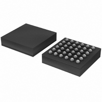
SC16C852SVIET,115 NXP Semiconductors, SC16C852SVIET,115 Datasheet - Page 14

SC16C852SVIET,115
Manufacturer Part Number
SC16C852SVIET,115
Description
IC UART DL 1.8V W/FIFO 36-TFBGA
Manufacturer
NXP Semiconductors
Datasheet
1.SC16C852SVIET151.pdf
(48 pages)
Specifications of SC16C852SVIET,115
Features
Programmable
Number Of Channels
2, DUART
Fifo's
128 Byte
Protocol
RS485
Voltage - Supply
1.8V
With Auto Flow Control
Yes
With Irda Encoder/decoder
Yes
With False Start Bit Detection
Yes
With Modem Control
Yes
With Cmos
Yes
Mounting Type
Surface Mount
Package / Case
36-TFBGA
Lead Free Status / RoHS Status
Lead free / RoHS Compliant
Other names
935286451115
SC16C852SVIET-G
SC16C852SVIET-G
SC16C852SVIET-G
SC16C852SVIET-G
Available stocks
Company
Part Number
Manufacturer
Quantity
Price
Company:
Part Number:
SC16C852SVIET,115
Manufacturer:
NXP Semiconductors
Quantity:
10 000
NXP Semiconductors
SC16C852SV_1
Product data sheet
6.10 Loopback mode
Table 6.
The internal loopback capability allows on-board diagnostics. In the Loopback mode, the
normal modem interface pins are disconnected and reconfigured for loopback internally
(see
In the Loopback mode, the transmitter output (TXA/TXB) and the receiver input
(RXA/RXB) are disconnected from their associated interface pins, and instead are
connected together internally. The CTSx, DSRx, CDx, and RIx are disconnected from
their normal modem control inputs pins, and instead are connected internally to RTS,
DTR, MCR[3] (OP2A/OP2B) and MCR[2] (OP1A/OP1B). Loopback test data is entered
into the transmit holding register via the user data bus interface, D[7:0]. The transmit
UART serializes the data and passes the serial data to the receive UART via the internal
loopback connection. The receive UART converts the serial data back into parallel data
that is then made available at the user data interface D[7:0]. The user optionally compares
the received data to the initial transmitted data for verifying error-free operation of the
UART TX/RX circuits.
In this mode the interrupt pins are 3-stated, therefore the software must use polling
method (see
Output
baud rate
(bit/s)
19.2 k
38.4 k
57.6 k
115.2 k
Figure
Baud rate generator programming table using a 1.8432 MHz clock with
MCR[7] = 0, SAMPR[1:0] = 00b and CLKPRE[3:0] = 0
7). MCR[3:0] register bits are used for controlling loopback diagnostic testing.
Section
Output
16 clock divisor
(decimal)
6
3
2
1
Dual UART with 128-byte FIFOs, IrDA, and XScale VLIO bus interface
Rev. 01 — 23 September 2008
7.2.2) to send and receive data.
Output
16 clock divisor
(hexadecimal)
06
03
02
01
DLM
program value
(hexadecimal)
00
00
00
00
SC16C852SV
…continued
© NXP B.V. 2008. All rights reserved.
DLL
program value
(hexadecimal)
06
03
02
01
14 of 48


