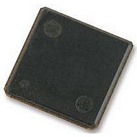
H5TQ2G63BFR-H9C HYNIX SEMICONDUCTOR, H5TQ2G63BFR-H9C Datasheet - Page 79

H5TQ2G63BFR-H9C
Manufacturer Part Number
H5TQ2G63BFR-H9C
Description
58T1898
Manufacturer
HYNIX SEMICONDUCTOR
Datasheet
1.H5TQ2G63BFR-H9C.pdf
(93 pages)
Specifications of H5TQ2G63BFR-H9C
Memory Type
SDRAM
Memory Configuration
128M X 16
Access Time
13.5ns
Interface Type
CMOS
Memory Case Style
FBGA
No. Of Pins
96
Operating Temperature Range
0°C To +85°C
Memory Size
2 Gbit
Rohs Compliant
Yes
Available stocks
Company
Part Number
Manufacturer
Quantity
Price
Company:
Part Number:
H5TQ2G63BFR-H9C
Manufacturer:
AD
Quantity:
1 001
Company:
Part Number:
H5TQ2G63BFR-H9C
Manufacturer:
HYNIX
Quantity:
9 500
Company:
Part Number:
H5TQ2G63BFR-H9C
Manufacturer:
HYNIX
Quantity:
4 000
Part Number:
H5TQ2G63BFR-H9C
Manufacturer:
HYNIX
Quantity:
20 000
Rev. 0.5 / Aug. 2010
Timing Parameter Notes
1. Actual value dependant upon measurement level definitions which are TBD.
2. Commands requiring a locked DLL are: READ (and RAP) and synchronous ODT commands.
3. The max values are system dependent.
4. WR as programmed in mode register.
5. Value must be rounded-up to next higher integer value.
6. There is no maximum cycle time limit besides the need to satisfy the refresh interval, tREFI.
7. tWR is defined in ns, for calculation of tWRPDEN it is necessary to round up tWR / tCK to the next integer.
8. WR in clock cycles as programmed in MR0.
9. The maximum postamble is bound by tHZDQS (max)
10. Output timing deratings are relative to the SDRAM input clock. When the device is operated with input clock jitter,
11. Value is only valid for RON34
12. Single ended signal parameter. Refer to chapter <t.b.d.> for definition and measurement method.
13. tREFI depends on TOPER
14. tIS (base) and tIH (base) values are for 1V/ns CMD/ADD single-ended slew rate and 2V/ns CK, CK differential slew
15. tDS (base) and tDH (base) values are for 1V/ns DQ single-ended slew rate and 2V/ns DQS, DQS differential slew rate.
16. Start of internal write transaction is definited as follows:
17. The maximum preamble is bound by tLZDQS (min)
18. CKE is allowed to be registered low while operations such as row activation, precharge, autoprecharge or refresh are
19. Although CKE is allowed to be registered LOW after a REFRESH command once tREFPDEN (min) is satisfied, there are
20. Defined between end of MPR read burst and MRS which reloads MPR or disables MPR function.
21. One ZQCS command can effectively correct a minimum of 0.5% (ZQCorrection) of RON and RTT impedance error
this parameter needs to be derated by t.b.d.
rate. Note for DQ and DM signals, VREF(DC) = VRefDQ (DC). For input only pins except RESET,
VRef (DC) = VRefCA (DC). See “Address / Command Setup, Hold and Derating” on page 80.
Note for DQ and DM signals, VREF(DC) = VRefDQ (DC). For input only pins except RESET, VRef (DC) = VRefCA (DC).
See “Data Setup, Hold and Slew Rate Derating” on page 87..
in progress, but power-down IDD spec will not be applied until finishing those operations.
Temperature Sensitivity’ and ‘ODT Voltage and Temperature Sensitivity’ tables. The appropriate interval between ZQCS
commands can be determined from these tables and other application specific parameters. One method for calculating
cases where additional time such as tXPDLL (min) is also required.
within 64 nCK for all speed bins assuming the maximum sensitivities specified in the ‘Output Driver Voltage and
the interval between ZQCS commands, given the temperature (Tdrifrate) and voltage (Vdriftrate) drift rates that the
SDRAM is subject to in the application, is illustrated. The interval could be defined by the following formula.
For BL8 (fixed by MRS and on- the-fly): Rising clock edge 4 clock cycles after WL.
For BC4 (on- the- fly): Rising clock edge 4 clock cycles after WL.
For BC4 (fixed by MRS): Rising clock edge 2 clock cycles after WL.
H5TQ2G63BFR
79


