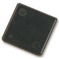
H5TQ2G63BFR-H9C HYNIX SEMICONDUCTOR, H5TQ2G63BFR-H9C Datasheet - Page 6

H5TQ2G63BFR-H9C
Manufacturer Part Number
H5TQ2G63BFR-H9C
Description
58T1898
Manufacturer
HYNIX SEMICONDUCTOR
Datasheet
1.H5TQ2G63BFR-H9C.pdf
(93 pages)
Specifications of H5TQ2G63BFR-H9C
Memory Type
SDRAM
Memory Configuration
128M X 16
Access Time
13.5ns
Interface Type
CMOS
Memory Case Style
FBGA
No. Of Pins
96
Operating Temperature Range
0°C To +85°C
Memory Size
2 Gbit
Rohs Compliant
Yes
Available stocks
Company
Part Number
Manufacturer
Quantity
Price
Company:
Part Number:
H5TQ2G63BFR-H9C
Manufacturer:
AD
Quantity:
1 001
Company:
Part Number:
H5TQ2G63BFR-H9C
Manufacturer:
HYNIX
Quantity:
9 500
Company:
Part Number:
H5TQ2G63BFR-H9C
Manufacturer:
HYNIX
Quantity:
4 000
Part Number:
H5TQ2G63BFR-H9C
Manufacturer:
HYNIX
Quantity:
20 000
1. DESCRIPTION
The H5TQ2G63BFR is a 2,147,483,648-bit CMOS Double Data Rate III (DDR3) Synchronous DRAM, ideally suited for the
main memory applications which requires large memory density and high bandwidth. Hynix 2Gb DDR3 SDRAMs offer fully
synchronous operations referenced to both rising and falling edges of the clock. While all addresses and control inputs are
latched on the rising edges of the CK (falling edges of the CK), Data, Data strobes and Write data masks inputs are sam-
pled on both rising and falling edges of it.
The data paths are internally pipelined and 8-bit prefetched to achieve very high bandwidth.
1.1 Device Features and Ordering Information
1.1.1 FEATURES
Rev. 0.5 / Aug. 2010
1.1.2 ORDERING INFORMATION
• VDD=VDDQ=1.5V +/- 0.075V
• Fully differential clock inputs (CK, CK) operation
• Differential Data Strobe (DQS, DQS)
• On chip DLL align DQ, DQS and DQS transition with CK
• DM masks write data-in at the both rising and falling
• All addresses and control inputs except data,
• Programmable CAS latency 6, 7, 8, 9, 10, 11 , 12, 13
• Programmable additive latency 0, CL-1, and CL-2
• Programmable CAS Write latency (CWL) = 5, 6, 7, 8, 9
• Programmable burst length 4/8 with both nibble
• BL switch on the fly
H5TQ2G63BFR-N0C
H5TQ2G63BFR-12C
H5TQ2G63BFR-11C
and 14 supported
transition
edges of the data strobe
data strobes and data masks latched on the
rising edges of the clock
supported
sequential and interleave mode
Part No.
VDD/VDDQ=1.5V
Power Supply
Frequency
800MHz
900MHz
1.0GHz
Clock
1.6Gbps/pin
1.8Gbps/pin
2.0Gbps/pin
Max Data
• 8banks
• Average Refresh Cycle (Tcase of 0
• Auto Self Refresh supported
• JEDEC standard 96ball FBGA(x16)
• Driver strength selected by EMRS
• Dynamic On Die Termination supported
• Asynchronous RESET pin supported
• ZQ calibration supported
• Write Levelization supported
• On Die Thermal Sensor supported
• 8 bit pre-fetch
Rate
- 7.8 µs at 0
- 3.9 µs at 85
o
Interface
C ~ 85
SSTL-15
o
C ~ 95
o
C
o
C
96ball FBGA
Package
o
C~ 95
H5TQ2G63BFR
o
C)
6


