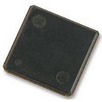
H5TQ2G63BFR-H9C HYNIX SEMICONDUCTOR, H5TQ2G63BFR-H9C Datasheet - Page 21

H5TQ2G63BFR-H9C
Manufacturer Part Number
H5TQ2G63BFR-H9C
Description
58T1898
Manufacturer
HYNIX SEMICONDUCTOR
Datasheet
1.H5TQ2G63BFR-H9C.pdf
(93 pages)
Specifications of H5TQ2G63BFR-H9C
Memory Type
SDRAM
Memory Configuration
128M X 16
Access Time
13.5ns
Interface Type
CMOS
Memory Case Style
FBGA
No. Of Pins
96
Operating Temperature Range
0°C To +85°C
Memory Size
2 Gbit
Rohs Compliant
Yes
Available stocks
Company
Part Number
Manufacturer
Quantity
Price
Company:
Part Number:
H5TQ2G63BFR-H9C
Manufacturer:
AD
Quantity:
1 001
Company:
Part Number:
H5TQ2G63BFR-H9C
Manufacturer:
HYNIX
Quantity:
9 500
Company:
Part Number:
H5TQ2G63BFR-H9C
Manufacturer:
HYNIX
Quantity:
4 000
Part Number:
H5TQ2G63BFR-H9C
Manufacturer:
HYNIX
Quantity:
20 000
Rev. 0.5 / Aug. 2010
1.9 Mode Register MR3
The Mode Register MR3 controls Multi purpose registers. The Mode Register 3 is written by asserting low on
CS, RAS, CAS, WE, high on BA1 and BA0, and low on BA2 while controlling the states of address pins
according to the table below.
MR3 Programming:
*1 : BA2, A3-A15 are RFU and must be programmed to 0 during MRS.
*2 : The predefined pattern will be used for read synchronization.
*3 : When MPr control is set for normal operation (MR3 A[2]=0) then MR3 A[1:0] will be ignored.
1.10 Multi-Purpose Register (MPR)
The Multi Purpose Register(MPR) function is used to Read out a predefined system timing calibration bit sequence. To
enable the MPR, a MODE Register Set(MRS) command must be issued to MR3 Register with bit A2=1. Prior to issuing
the MRS command, all banks must be in the idle state (all banks precharged and tRP met). Once the MPR is enabled,
any subsequent RD or RDA commands will be redirected to the Multi Purpose Register. When the MPR is enabled, only
RD ro RDA commands are allowed until a subsequent MRS command is issued with the MPR disabled(MR3 bit A2=0).
Power-Down mode, Self-Refresh, and any other non-RD/RDA command is not allowed during MPR enable mode. The
RESET function is supported during MPR enable mode. For detailed MPR operation refer to “Multi Purpose Register”.
BA
0*
BA1
1
2
0
0
1
1
BA
1
1
BA
1
BA0
0
1
0
1
0
A
15 ~
A
13
A
12
MR Select
MPR Operation
A
MR0
MR1
MR2
MR3
11
0
1
A2
A
10
Dataflow from MPR
A
Normal operation*
9
Figure 9. MR3 Definition
0*
A
MPR*
1
8
2
A
7
3
A
6
A
5
MPR Address
A1
A
0
0
1
1
4
A
A0
0
1
0
1
3
MPR
A
2
Predefined pattern*
A
MPR Loc
1
MPR location
A
RFU
RFU
RFU
0
H5TQ2G63BFR
Mode Register 3
Address Field
2
21


