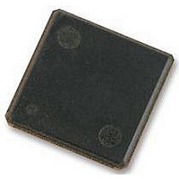
H5TQ2G63BFR-H9C HYNIX SEMICONDUCTOR, H5TQ2G63BFR-H9C Datasheet - Page 13

H5TQ2G63BFR-H9C
Manufacturer Part Number
H5TQ2G63BFR-H9C
Description
58T1898
Manufacturer
HYNIX SEMICONDUCTOR
Datasheet
1.H5TQ2G63BFR-H9C.pdf
(93 pages)
Specifications of H5TQ2G63BFR-H9C
Memory Type
SDRAM
Memory Configuration
128M X 16
Access Time
13.5ns
Interface Type
CMOS
Memory Case Style
FBGA
No. Of Pins
96
Operating Temperature Range
0°C To +85°C
Memory Size
2 Gbit
Rohs Compliant
Yes
Available stocks
Company
Part Number
Manufacturer
Quantity
Price
Company:
Part Number:
H5TQ2G63BFR-H9C
Manufacturer:
AD
Quantity:
1 001
Company:
Part Number:
H5TQ2G63BFR-H9C
Manufacturer:
HYNIX
Quantity:
9 500
Company:
Part Number:
H5TQ2G63BFR-H9C
Manufacturer:
HYNIX
Quantity:
4 000
Part Number:
H5TQ2G63BFR-H9C
Manufacturer:
HYNIX
Quantity:
20 000
Rev. 0.5 / Aug. 2010
1.6 Mode Register MR0
The mode register stores the data for controlling the various operating modes of DDR3 SDRAM. It controls
burst length, read burst type, CAS latency, test mode, DLl reset, WR and DLL control for precharge Power-
Down, which include various vendor specific options to make DDR3 SDRAM useful for various applicatons.
The mode register is written by asserting low on CS, CAS, WE, BA0, BA1, and BA2, while controlling the
states of address pins according to Figure 6.
*1 : BA2 and A13~A15 are RFU and must be programmed to 0 during MRS.
*2: WR(write recovery for autoprecharge) min in clock cycles is calculated by dividing tWR(in ns) by tCK(in ns) and rounding up to the next
integer: WRmin[cycles] = Roundup(tWR[ns]/tCK[ns]). The WR value in the mode register must be programmed to be equal or larger than
WRmin. The programmed WR value is used with tRP to determine tDAL.
*3: The table only shows the encodings for a given Cas Latency. For actual supported Cas Latency, please refer to speedbin tables for each
frequency.
*4: The table only shows the encodings for Write Recovery. For actual Write recovery timing, please refer to AC timing table.
BA1
0
0
1
1
A12
0
1
BA
0*
1
BA0
2
0
1
0
1
BA
0
DLL Control for
Precharge PD
Slow exit (DLL off)
Fast exit (DLL on)
A8
1
0
1
BA
0
0
MR Select
MR0
MR1
MR2
MR3
DLL Reset
A
15
~ A
0*
Yes
No
1
13
PPD
A
Figure 6. DDR3 SDRAM mode register set (MR0)
12
A
Write recovery for autoprecharge
11
A11
0
0
0
0
1
1
1
1
A
WR
10
A7
A10
0
0
1
1
0
0
1
1
A
0
1
9
DLL
A
0
1
0
1
0
1
0
1
8
A9
mode
Normal
TM
Test
A
7
WR(cycles)
A
CAS Latency
6
16
10
12
14
8
5
6
7
*2
*2
*2
*2
*2
*2
*2
*2
A
5
0
1
A3
A
4
RBT
Read Burst Type
A
3
Sequential
Interleave
A
CL
A6
0
0
0
0
1
1
1
1
0
0
0
2
A
1
A5
BL
0
0
1
1
0
0
1
1
0
0
1
A
0
A4
0
1
0
1
0
1
0
1
0
1
0
0
0
0
0
1
1
1
1
A2
A1
Address Field
Mode Register 0
H5TQ2G63BFR
0
0
0
0
0
0
0
0
1
1
1
A2
A1
A0
1
1
1
1
0
0
1
1
BC4 of 8(on the fly)
BC4 of 8(on the fly)
CAS Latency
BL
BL
BC4 (Fixed)
BC4 (Fixed)
Reserved
Reserved
Reserved
8 (Fixed)
8 (Fixed)
10
11
12
13
14
5
6
7
8
9
13


