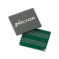
MT48LC8M32B2B5-6 Micron Technology Inc, MT48LC8M32B2B5-6 Datasheet - Page 25

MT48LC8M32B2B5-6
Manufacturer Part Number
MT48LC8M32B2B5-6
Description
Manufacturer
Micron Technology Inc
Type
SDRAMr
Datasheet
1.MT48LC8M32B2B5-6.pdf
(56 pages)
Specifications of MT48LC8M32B2B5-6
Organization
8Mx32
Density
256Mb
Address Bus
14b
Access Time (max)
17/7.5/5.5ns
Maximum Clock Rate
166MHz
Operating Supply Voltage (typ)
3.3V
Package Type
FBGA
Operating Temp Range
0C to 70C
Operating Supply Voltage (max)
3.6V
Operating Supply Voltage (min)
3V
Supply Current
165mA
Pin Count
90
Mounting
Surface Mount
Operating Temperature Classification
Commercial
Lead Free Status / Rohs Status
Compliant
Available stocks
Company
Part Number
Manufacturer
Quantity
Price
Company:
Part Number:
MT48LC8M32B2B5-6 TR
Manufacturer:
Micron Technology Inc
Quantity:
10 000
CLOCK SUSPEND
The clock suspend mode occurs when a column
access/burst is in progress and CKE is registered LOW.
In the clock suspend mode, the internal clock is deacti-
vated, freezing the synchronous logic.
For each positive clock edge on which CKE is sampled
LOW, the next internal positive clock edge is sus-
pended. Any command or data present on the input
pins at the time of a suspended internal clock edge is
ignored. Any data present on the DQ pins remains
driven. Also, burst counters are not incremented, as
long as the clock is suspended. (See examples in Fig-
ures 25 and 26.)
Clock suspend mode is exited by registering CKE
HIGH; the internal clock and related operation will
resume on the subsequent positive clock edge.
NOTE:
09005aef8140ad6d
MT48LC8M32B2_2.fm - Rev. B 10/04 EN
COMMAND
CLK
CKE
For this example, BL = 4 or greater, and DM is LOW.
Figure 25: CLOCK SUSPEND During
All banks idle
Enter power-down mode
COMMAND
INTERNAL
ADDRESS
CLOCK
CKE
CLK
D
t CKS
IN
Figure 24: Power-Down
NOP
NOP
T0
Input buffers gated off
WRITE Burst
BANK,
WRITE
COL n
T1
D
n
IN
(
(
(
(
)
)
(
)
)
)
T2
(
(
(
)
)
(
)
(
)
)
Exit power-down mode
T3
> t CKS
NOP
n + 1
T4
D
IN
NOP
DON’T CARE
T5
NOP
n + 2
D
IN
DON’T CARE
ACTIVE
t RCD
t RAS
t RC
25
NOTE:
BURST READ/SINGLE WRITE
The burst read/single write mode is entered by pro-
gramming the write burst mode bit (M9) in the mode
register to a logic “1.” In this mode, all WRITE com-
mands result in the access of a single column location
(burst of one), regardless of the programmed burst
length. READ commands access columns according to
the programmed burst length and sequence, just as in
the normal mode of operation (M9 = 0).
CONCURRENT AUTO PRECHARGE
An access command to (READ or WRITE) another
bank while an access command with auto precharge
enabled is executing is not allowed by SDRAMs, unless
the SDRAM supports CONCURRENT AUTO PRE-
CHARGE. Micron SDRAMs support CONCURRENT
AUTO PRECHARGE. Four cases where CONCURRENT
AUTO PRECHARGE occurs are defined below.
READ with AUTO PRECHARGE
1. Interrupted by a READ (with or without auto pre-
charge): A READ to bank m will interrupt a READ on
bank n, CAS latency later. The PRECHARGE to bank n
will begin when the READ to bank m is registered
(Figure 27).
2. Interrupted by a WRITE (with or without auto pre-
charge): A WRITE to bank m will interrupt a READ on
bank n when registered. DQM should be used two
clocks prior to the WRITE command to prevent bus
contention. The PRECHARGE to bank n will begin
when the WRITE to bank m is registered (Figure 28).
COMMAND
INTERNAL
ADDRESS
For this example, CL = 2, BL = 4 or greater, and DQM is
LOW.
Figure 26: CLOCK SUSPEND During
CLOCK
CLK
CKE
Micron Technology, Inc., reserves the right to change products or specifications without notice.
DQ
T0
BANK,
READ
COL n
T1
NOP
READ Burst
T2
NOP
D
OUT
n
T3
©2003 Micron Technology, Inc. All rights reserved.
256Mb: x32
n + 1
D
OUT
T4
NOP
SDRAM
T5
NOP
n + 2
D
OUT
DON’T CARE
T6
NOP
D
n + 3
OUT


