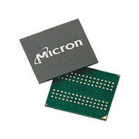
MT48LC8M32B2B5-6 Micron Technology Inc, MT48LC8M32B2B5-6 Datasheet - Page 16

MT48LC8M32B2B5-6
Manufacturer Part Number
MT48LC8M32B2B5-6
Description
Manufacturer
Micron Technology Inc
Type
SDRAMr
Datasheet
1.MT48LC8M32B2B5-6.pdf
(56 pages)
Specifications of MT48LC8M32B2B5-6
Organization
8Mx32
Density
256Mb
Address Bus
14b
Access Time (max)
17/7.5/5.5ns
Maximum Clock Rate
166MHz
Operating Supply Voltage (typ)
3.3V
Package Type
FBGA
Operating Temp Range
0C to 70C
Operating Supply Voltage (max)
3.6V
Operating Supply Voltage (min)
3V
Supply Current
165mA
Pin Count
90
Mounting
Surface Mount
Operating Temperature Classification
Commercial
Lead Free Status / Rohs Status
Compliant
Available stocks
Company
Part Number
Manufacturer
Quantity
Price
Company:
Part Number:
MT48LC8M32B2B5-6 TR
Manufacturer:
Micron Technology Inc
Quantity:
10 000
READs
READ bursts are initiated with a READ command, as
shown in Figure 8.
The starting column and bank addresses are provided
with the READ command, and auto precharge is either
enabled or disabled for that burst access. If auto pre-
charge is enabled, the row being accessed is pre-
charged at the completion of the burst. For the generic
READ commands used in the following illustrations,
auto precharge is disabled.
During READ bursts, the valid data-out element from
the starting column address will be available following
the CAS latency after the READ command. Each subse-
quent data-out element will be valid by the next posi-
tive clock edge. Figure 9 shows general timing for each
possible CAS latency setting.
Upon completion of a burst, assuming no other com-
mands have been initiated, the DQs will go High-Z. A
full-page burst will continue until terminated. (At the
end of the page, it will wrap to column 0 and continue.)
Data from any READ burst may be truncated with a
subsequent READ command, and data from a fixed-
length READ burst may be immediately followed by
data from a READ command.
In either case, a continuous flow of data can be main-
tained. The first data element from the new burst fol-
lows either the last element of a completed burst or the
last desired data element of a longer burst that is being
truncated. The new READ command should be issued
x cycles before the clock edge at which the last desired
data element is valid, where x equals the CAS latency
minus one. This is shown in Figure 10 for CAS latencies
of one, two and three; data element n + 3 is either the
last of a burst of four or the last desired of a longer
burst. SDRAMs use a pipelined architecture and there-
fore does not require the 2n rule associated with a
prefetch architecture. A READ command can be initi-
ated on any clock cycle following a previous READ
command. Full-speed random read accesses can be
performed to the same bank, as shown in Figure 11, or
each subsequent READ may be performed to a differ-
ent bank.
09005aef8140ad6d
MT48LC8M32B2_2.fm - Rev. B 10/04 EN
16
COMMAND
COMMAND
COMMAND
Micron Technology, Inc., reserves the right to change products or specifications without notice.
CLK
CLK
CLK
DQ
DQ
DQ
A8, A9, A11
Figure 8: READ Command
Figure 9: CAS Latency
A0-A7
BA0,1
RAS#
CAS#
READ
READ
WE#
READ
T0
T0
CKE
A10
CLK
T0
CS#
CL = 1
t
t AC
LZ
HIGH
CL = 2
NOP
NOP
T1
NOP
T1
T1
t
t AC
LZ
CL = 3
D
t OH
OUT
ENABLE AUTO PRECHARGE
DISABLE AUTO PRECHARGE
©2003 Micron Technology, Inc. All rights reserved.
COLUMN
ADDRESS
ADDRESS
BANK
T2
NOP
T2
NOP
T2
t
t AC
LZ
D
256Mb: x32
t OH
OUT
DON’T CARE
SDRAM
T3
T3
NOP
D
t OH
OUT
DON’T CARE
UNDEFINED
T4


