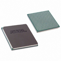
EP1S20F780I6N Altera, EP1S20F780I6N Datasheet - Page 458

EP1S20F780I6N
Manufacturer Part Number
EP1S20F780I6N
Description
IC STRATIX FPGA 20K LE 780-FBGA
Manufacturer
Altera
Series
Stratix®r
Specifications of EP1S20F780I6N
Number Of Logic Elements/cells
18460
Number Of Labs/clbs
1846
Total Ram Bits
1669248
Number Of I /o
586
Voltage - Supply
1.425 V ~ 1.575 V
Mounting Type
Surface Mount
Operating Temperature
-40°C ~ 100°C
Package / Case
780-FBGA
Family Name
Stratix
Number Of Logic Blocks/elements
18460
# I/os (max)
586
Frequency (max)
450.05MHz
Process Technology
0.13um (CMOS)
Operating Supply Voltage (typ)
1.5V
Logic Cells
18460
Ram Bits
1669248
Operating Supply Voltage (min)
1.425V
Operating Supply Voltage (max)
1.575V
Operating Temp Range
-40C to 100C
Operating Temperature Classification
Industrial
Mounting
Surface Mount
Pin Count
780
Package Type
FC-FBGA
Lead Free Status / RoHS Status
Lead free / RoHS Compliant
Number Of Gates
-
Lead Free Status / Rohs Status
Compliant
Available stocks
Company
Part Number
Manufacturer
Quantity
Price
Company:
Part Number:
EP1S20F780I6N
Manufacturer:
ALTERA
Quantity:
3 000
- Current page: 458 of 864
- Download datasheet (11Mb)
I/O Pad Placement Guidelines
I/O Pad
Placement
Guidelines
4–30
Stratix Device Handbook, Volume 2
Differential termination for Stratix devices is supported for the left and
right I/O banks. Differential termination for Stratix GX devices is
supported for the left, source-synchronous I/O bank. Some of the clock
input pins are in the top and bottom I/O banks, which do not support
differential termination. Clock pins CLK[1,3,8,10] support differential
on-chip termination. Clock pins CLK[0,2,9,11], CLK[4-7], and CLK[12-15]
do not support differential on-chip termination.
Transceiver Termination
Stratix GX devices feature built-in on-chip termination within the
transceiver at both the transmit and receive buffers. This termination
improves signal integrity and provides support for the 1.5-V PCML I/O
standard.
This section provides pad placement guidelines for the programmable
I/O standards supported by Stratix and Stratix GX devices and includes
essential information for designing systems using the devices' selectable
I/O capabilities. These guidelines will reduce noise problems so that
FPGA devices can maintain an acceptable noise level on the line from the
V
each bank, these noise issues do not have any effect when crossing bank
boundaries and these guidelines do not apply. Although pad placement
rules need not be considered between I/O banks, some rules must be
considered if you are using a VREF signal in a PLLOUT bank. Note that the
signals in the PLLOUT banks share the V
banks and, therefore, must adhere to the V
Pad Placement
Differential Pad Placement Guidelines
To avoid cross coupling and maintain an acceptable noise level on the
V
pads in relation to differential pads. Use the following guidelines for
placing single-ended pads with respect to differential pads in Stratix
devices. These guidelines apply for LVDS, HyperTransport technology,
LVPECL, and PCML I/O standards. The differential pad placement
guidelines do not apply for differential HSTL and differential SSTL
output clocks since each differential output clock is essentially
implemented using two single-ended output buffers. These rules do not
apply to differential HSTL input clocks either even though the dedicated
input buffers are used. However, both differential HSTL and differential
SSTL output standards must adhere to the single-ended (VREF) pad
placement restrictions discussed in
CCIO
CCIO
supply, there are restrictions on the placement of single-ended I/O
supply. Since Altera FPGAs require that a separate V
Guidelines”.
“VREF Pad Placement
REF
REF
supply with neighboring I/O
rules discussed in
Altera Corporation
Guidelines”.
CCIO
June 2006
power
“VREF
Related parts for EP1S20F780I6N
Image
Part Number
Description
Manufacturer
Datasheet
Request
R

Part Number:
Description:
CYCLONE II STARTER KIT EP2C20N
Manufacturer:
Altera
Datasheet:

Part Number:
Description:
CPLD, EP610 Family, ECMOS Process, 300 Gates, 16 Macro Cells, 16 Reg., 16 User I/Os, 5V Supply, 35 Speed Grade, 24DIP
Manufacturer:
Altera Corporation
Datasheet:

Part Number:
Description:
CPLD, EP610 Family, ECMOS Process, 300 Gates, 16 Macro Cells, 16 Reg., 16 User I/Os, 5V Supply, 15 Speed Grade, 24DIP
Manufacturer:
Altera Corporation
Datasheet:

Part Number:
Description:
Manufacturer:
Altera Corporation
Datasheet:

Part Number:
Description:
CPLD, EP610 Family, ECMOS Process, 300 Gates, 16 Macro Cells, 16 Reg., 16 User I/Os, 5V Supply, 30 Speed Grade, 24DIP
Manufacturer:
Altera Corporation
Datasheet:

Part Number:
Description:
High-performance, low-power erasable programmable logic devices with 8 macrocells, 10ns
Manufacturer:
Altera Corporation
Datasheet:

Part Number:
Description:
High-performance, low-power erasable programmable logic devices with 8 macrocells, 7ns
Manufacturer:
Altera Corporation
Datasheet:

Part Number:
Description:
Classic EPLD
Manufacturer:
Altera Corporation
Datasheet:

Part Number:
Description:
High-performance, low-power erasable programmable logic devices with 8 macrocells, 10ns
Manufacturer:
Altera Corporation
Datasheet:

Part Number:
Description:
Manufacturer:
Altera Corporation
Datasheet:

Part Number:
Description:
Manufacturer:
Altera Corporation
Datasheet:

Part Number:
Description:
Manufacturer:
Altera Corporation
Datasheet:

Part Number:
Description:
CPLD, EP610 Family, ECMOS Process, 300 Gates, 16 Macro Cells, 16 Reg., 16 User I/Os, 5V Supply, 25 Speed Grade, 24DIP
Manufacturer:
Altera Corporation
Datasheet:


