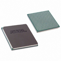
EP1S20F780I6N Altera, EP1S20F780I6N Datasheet - Page 452

EP1S20F780I6N
Manufacturer Part Number
EP1S20F780I6N
Description
IC STRATIX FPGA 20K LE 780-FBGA
Manufacturer
Altera
Series
Stratix®r
Specifications of EP1S20F780I6N
Number Of Logic Elements/cells
18460
Number Of Labs/clbs
1846
Total Ram Bits
1669248
Number Of I /o
586
Voltage - Supply
1.425 V ~ 1.575 V
Mounting Type
Surface Mount
Operating Temperature
-40°C ~ 100°C
Package / Case
780-FBGA
Family Name
Stratix
Number Of Logic Blocks/elements
18460
# I/os (max)
586
Frequency (max)
450.05MHz
Process Technology
0.13um (CMOS)
Operating Supply Voltage (typ)
1.5V
Logic Cells
18460
Ram Bits
1669248
Operating Supply Voltage (min)
1.425V
Operating Supply Voltage (max)
1.575V
Operating Temp Range
-40C to 100C
Operating Temperature Classification
Industrial
Mounting
Surface Mount
Pin Count
780
Package Type
FC-FBGA
Lead Free Status / RoHS Status
Lead free / RoHS Compliant
Number Of Gates
-
Lead Free Status / Rohs Status
Compliant
Available stocks
Company
Part Number
Manufacturer
Quantity
Price
Company:
Part Number:
EP1S20F780I6N
Manufacturer:
ALTERA
Quantity:
3 000
- Current page: 452 of 864
- Download datasheet (11Mb)
Stratix & Stratix GX I/O Banks
4–24
Stratix Device Handbook, Volume 2
Non-Voltage-Referenced Standards
Each Stratix I/O bank has its own VCCIO pins and supports only one
V
support any number of input signals with different I/O standard
assignments, as shown in
For output signals, a single I/O bank can only support non-voltage-
referenced output signals driving at the same voltage as V
I/O bank can only have one V
value for non-voltage referenced signals. For example, an I/O bank with
a 2.5-V V
HyperTransport technology inputs and outputs, and 3.3-V LVCMOS
inputs (not output or bidirectional pins).
1
Voltage-Referenced Standards
To accommodate voltage-referenced I/O standards, each Stratix I/O
bank supports multiple VREF pins feeding a common VREF bus. The
number of available VREF pins increases as device density increases. If
these pins are not used as VREF pins, they can not be used as generic I/O
pins.
Notes to
(1)
(2)
3.3 V
2.5 V
1.8 V
1.5 V
Table 4–5. Acceptable Input Levels for LVTTL/LVCMOS
CCIO
Bank V
Because the input signal will not drive to the rail, the input buffer does not
completely shut off, and the I/O current will be slightly higher than the default
value.
These input values overdrive the input buffer, so the pin leakage current will be
slightly higher than the default value.
, either 1.5, 1.8, 2.5 or 3.3 V. A Stratix I/O bank can simultaneously
Table
If the output buffer overdrives the input buffer, you must turn
on the Allow voltage overdrive for LVTTL/LVCMOS option in
the Quartus II software. To see this option, click the Device &
Pin Options button in the Device page of the Settings dialog
box (Assignments menu). Then click the Pin Placement tab in
the Device & Pin Options dialog box.
CCIO
CCIO
setting can support 2.5-V LVTTL inputs and outputs,
4–5:
v
v
3.3 V
v
v
(2)
(2)
Table
CCIO
4–5.
Acceptable Input Levels
v
v
2.5 V
value, so it can only drive out that one
v
v
(2)
(2)
1.8 V
v
v
Altera Corporation
CCIO
. A Stratix
June 2006
v
1.5 V
v
(1)
Related parts for EP1S20F780I6N
Image
Part Number
Description
Manufacturer
Datasheet
Request
R

Part Number:
Description:
CYCLONE II STARTER KIT EP2C20N
Manufacturer:
Altera
Datasheet:

Part Number:
Description:
CPLD, EP610 Family, ECMOS Process, 300 Gates, 16 Macro Cells, 16 Reg., 16 User I/Os, 5V Supply, 35 Speed Grade, 24DIP
Manufacturer:
Altera Corporation
Datasheet:

Part Number:
Description:
CPLD, EP610 Family, ECMOS Process, 300 Gates, 16 Macro Cells, 16 Reg., 16 User I/Os, 5V Supply, 15 Speed Grade, 24DIP
Manufacturer:
Altera Corporation
Datasheet:

Part Number:
Description:
Manufacturer:
Altera Corporation
Datasheet:

Part Number:
Description:
CPLD, EP610 Family, ECMOS Process, 300 Gates, 16 Macro Cells, 16 Reg., 16 User I/Os, 5V Supply, 30 Speed Grade, 24DIP
Manufacturer:
Altera Corporation
Datasheet:

Part Number:
Description:
High-performance, low-power erasable programmable logic devices with 8 macrocells, 10ns
Manufacturer:
Altera Corporation
Datasheet:

Part Number:
Description:
High-performance, low-power erasable programmable logic devices with 8 macrocells, 7ns
Manufacturer:
Altera Corporation
Datasheet:

Part Number:
Description:
Classic EPLD
Manufacturer:
Altera Corporation
Datasheet:

Part Number:
Description:
High-performance, low-power erasable programmable logic devices with 8 macrocells, 10ns
Manufacturer:
Altera Corporation
Datasheet:

Part Number:
Description:
Manufacturer:
Altera Corporation
Datasheet:

Part Number:
Description:
Manufacturer:
Altera Corporation
Datasheet:

Part Number:
Description:
Manufacturer:
Altera Corporation
Datasheet:

Part Number:
Description:
CPLD, EP610 Family, ECMOS Process, 300 Gates, 16 Macro Cells, 16 Reg., 16 User I/Os, 5V Supply, 25 Speed Grade, 24DIP
Manufacturer:
Altera Corporation
Datasheet:


