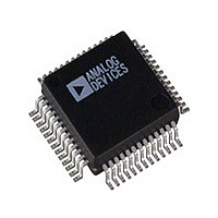
ADV7196AKSZ Analog Devices Inc, ADV7196AKSZ Datasheet - Page 4

ADV7196AKSZ
Manufacturer Part Number
ADV7196AKSZ
Description
Manufacturer
Analog Devices Inc
Datasheet
1.ADV7196AKSZ.pdf
(36 pages)
Specifications of ADV7196AKSZ
Adc/dac Resolution
11b
Screening Level
Commercial
Package Type
MQFP
Pin Count
52
Lead Free Status / RoHS Status
Compliant
ADV7196A–SPECIFICATIONS
3.3 V SPECIFICATIONS
Parameter
STATIC PERFORMANCE
DIGITAL OUTPUTS
DIGITAL AND CONTROL INPUTS
ANALOG OUTPUTS
VOLTAGE REFERENCE (External)
POWER REQUIREMENTS
NOTES
1
2
3
4
Specifications subject to change without notice.
3 V DYNAMIC–SPECIFICATIONS
Parameter
Luma Bandwidth
Chroma Bandwidth
Signal-to-Noise Ratio
Chroma/Luma Delay Inequality
Specifications subject to change without notice.
Guaranteed by characterization.
I
I
All DACs on.
DD
AA
Resolution (Each DAC)
Integral Nonlinearity
Differential Nonlinearity
Output High Voltage, V
Output Low Voltage, V
Three State Leakage Current
Three State Output Capacitance
Input High Voltage, V
Input Low Voltage, V
Input Current, I
Input Capacitance, C
Full-Scale Output Current
Output Current Range
Full-Scale Output Current
Output Current Range
DAC-to-DAC Matching
Output Compliance Range, V
Output Impedance, R
Output Capacitance, C
Reference Range, V
I
I
I
I
I
Power Supply Rejection Ratio
DD
DD
DD
AA
PLL
is the total current required to supply all DACs including the V
or the circuit current is the continuous current required to drive the digital core without I
3, 4
2
2
2
IN
REF
IN
IL
OUT
IH
OUT
OH
OL
OC
(V
(0 C to 70 C) unless otherwise noted.)
AA
= 3.15 V to 3.45 V, V
Min
(V
T
MIN
AA
to T
Min
2.4
2
3.92
3.92
2.54
2.39
0
1.112
= 3.15 V to 3.45 V, V
REF
MAX
circuitry.
REF
(0 C to 70 C) unless otherwise noted.)
= 1.235 V, R
Typ
11
1.5
0.9
4
0.8
0
4
4.25
4.25
2.83
2.66
1.4
1.4
100
7
1.235
25
51
40
11
6.0
0.01
Typ
13.5
6.75
64
0
REF
SET
PLL
= 1.235 V, R
= 2470
.
1.359
12
Max
2.0
0.4
10
0.65
1
4.56
4.56
3.11
2.93
35
60
15
, R
SET
Max
LOAD
= 2470
Unit
Bits
LSB
LSB
V
V
µA
pF
V
V
µA
pF
mA
mA
mA
mA
%
V
kΩ
pF
V
mA
mA
mA
mA
mA
%/%
= 300
, R
. All specifications T
LOAD
Test Conditions
I
I
V
V
DAC A
DAC A
DAC B, C
DAC B, C
1× Interpolation
2× Interpolation
HDTV Mode
(with f
1× Interpolation, 2× Interpola-
tion, and HDTV Mode
1× Interpolation, 2× Interpola-
tion, and HDTV Mode
SINK
SOURCE
IN
IN
Unit
MHz
MHz
dB Luma Ramp Unweighted
ns
= 300
= 0.0 V or V
= 0.4 V
= 3.2 mA
CLK
= 400 µA
= 74.25 MHz)
. All specifications
DD
MIN
to T
MAX


