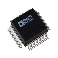
ADV7196AKSZ Analog Devices Inc, ADV7196AKSZ Datasheet - Page 31

ADV7196AKSZ
Manufacturer Part Number
ADV7196AKSZ
Description
Manufacturer
Analog Devices Inc
Datasheet
1.ADV7196AKSZ.pdf
(36 pages)
Specifications of ADV7196AKSZ
Adc/dac Resolution
11b
Screening Level
Commercial
Package Type
MQFP
Pin Count
52
Lead Free Status / RoHS Status
Compliant
DAC output traces on a PCB should be treated as transmission
lines. It is recommended that the DACs be placed as close as
possible to the output connector, with the analog output traces
being as short as possible (less than 3 inches). The DAC termina-
tion resistors should be placed as close as possible to the DAC
outputs and should overlay the PCB’s ground plane. As well as
minimizing reflections, short analog output traces will reduce noise
pickup due to neighboring digital circuitry
Supply Decoupling
Noise on the analog power plane can be further reduced by the
use of decoupling capacitors.
Optimum performance is achieved by the use of 0.1 µF ceramic
capacitors. Each of group of V
vidually decoupled to ground. This should be done by placing
the capacitors as close as possible to the device with the capaci-
tor leads as short as possible, thus minimizing lead inductance
Digital Signal Interconnect
The digital signal lines should be isolated as much as possible
from the analog outputs and other analog circuitry. Digital signal
lines should not overlay the analog power plane.
ADV7196A
DAC A
DAC B
DAC C
AA
or V
DD
.
pins should be indi-
LPF
LPF
LPF
AD8057
AD8057
AD8057
.
+5V
–5V
+5V
–5V
+5V
+5V
Due to the high clock rates used, long clock lines to the ADV7196A
should be avoided to minimize noise pickup. Any active pull-up
termination resistors for the digital inputs should be connected
to the digital power plane and not the analog power plane
Analog Signal Interconnect
The ADV7196A should be located as close as possible to the output
connectors thus minimizing noise pickup and reflections due to
impedance mismatch.
For optimum performance, the analog outputs should each have
a source termination resistance to ground of 75 Ω. This termina-
tion resistance should be as close as possible to the ADV7196A
to minimize reflections.
Any unused inputs should be tied to ground
Video Output Buffer and Optional Output Filter
Output buffering is necessary in order to drive output devices
such as progressive scan or HDTV monitors
Analog Devices produces a range of suitable op amps for this
application. Suitable op amps would be the AD8009, AD8002,
AD8001, or AD8057. More information on line driver buffering
circuits is given in the relevant op amp data sheets.
0.1 F
0.1 F
0.1 F
75
75
75
0.1 F
0.1 F
0.1 F
10 F
10 F
10 F
75
75
75
COAX
COAX
COAX
10 F
10 F
10 F
75
75
75
PROGRESSIVE
MONITOR
SCAN
.
ADV7196A
.
.
,


