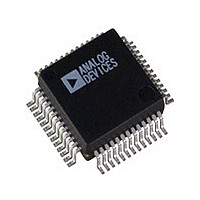
ADV7196AKSZ Analog Devices Inc, ADV7196AKSZ Datasheet - Page 28

ADV7196AKSZ
Manufacturer Part Number
ADV7196AKSZ
Description
Manufacturer
Analog Devices Inc
Datasheet
1.ADV7196AKSZ.pdf
(36 pages)
Specifications of ADV7196AKSZ
Adc/dac Resolution
11b
Screening Level
Commercial
Package Type
MQFP
Pin Count
52
Lead Free Status / RoHS Status
Compliant
ADV7196A
MODE REGISTER 2
MR1 (MR27–MR20)
(Address (SR4–SR0) = 02H)
Figure 53 shows the various operations under the control of Mode
Register 2.
MR2 BIT DESCRIPTION
Y Delay (MR20–MR22)
With these bits it is possible to delay the Y signal with respect to
the falling edge of the horizontal sync signal by up to four pixel
clock cycles. Figure 52 demonstrates this facility.
Color Delay (MR23–MR25)
With theses bits it is possible to delay the color signals with respect
to the falling edge of the horizontal sync signal by up to four pixel
clock cycles. Figure 52 demonstrates this facility.
Reserved (MR26–MR27)
A “0” must be written to these bits
PrPb DELAY
Y DELAY
NO DELAY
NO DELAY
MAX DELAY
MAX DELAY
ZERO MUST BE
MR37–MR36
WRITTEN TO
THESE BITS
MR37
MR27
.
ZERO MUST BE
WRITTEN TO
MR27–MR26
THESE BITS
MR36
MR26
Y OUTPUT
PrPb OUTPUTS
MR35
0
1
MR35
MR25
DAC C CONTROL
MR25 MR24 MR23
0
0
0
0
1
MR34
0
1
POWER-DOWN
NORMAL
DAC B CONTROL
0
0
1
1
0
MR34
MR24
COLOR DELAY
POWER-DOWN
NORMAL
0
1
0
1
0
MODE REGISTER 3
MR3 (MR37–MR30)
(Address (SR4-SR0) = 03H)
Figure 54 shows the various operations under the control of Mode
Register 3
MR3 BIT DESCRIPTION
HDTV Enable (MR30)
When this bit is set to “1” the ADV7196A reverts to HDTV
mode. When set to “0” the ADV7196A reverts to Progressive
Scan mode (PS mode).
Reserved (MR31–MR32)
A “0” must be written to these bits.
DAC A Control (MR33)
Setting this bit to “1” enables DAC A, otherwise this DAC is
powered down.
DAC B Control (MR34)
Setting this bit to “1” enables DAC B, otherwise this DAC is
powered down.
DAC C Control (MR35)
Setting this bit to “1” enables DAC C, otherwise this DAC is
powered down.
Reserved (MR36–MR37)
A “0” must be written to these bits.
MR23
MR33
MR33
0
1
DAC A CONTROL
0 PCLK
1 PCLK
2 PCLK
3 PCLK
4 PCLK
POWER-DOWN
NORMAL
ZERO MUST BE
MR32–MR31
WRITTEN TO
THESE BITS
MR32
.
MR22
MR22 MR21 MR20
0
0
0
0
1
0
0
1
1
0
MR31
MR21
Y DELAY
0
1
0
1
0
MR30
0
1
HDTV ENABLE
MR20
MR30
0 PCLK
1 PCLK
2 PCLK
3 PCLK
4 PCLK
DISABLE
ENABLE


