ATF-521P8-TR1 Avago Technologies US Inc., ATF-521P8-TR1 Datasheet - Page 3
ATF-521P8-TR1
Manufacturer Part Number
ATF-521P8-TR1
Description
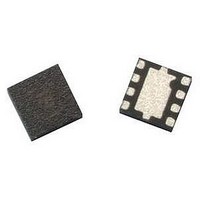
IC PHEMT 2GHZ 4.5V 200MA 8-LPCC
Manufacturer
Avago Technologies US Inc.
Datasheet
1.ATF-521P8-BLK.pdf
(23 pages)
Specifications of ATF-521P8-TR1
Gain
17dB
Transistor Type
pHEMT FET
Frequency
2GHz
Voltage - Rated
7V
Current Rating
500mA
Noise Figure
1.5dB
Current - Test
200mA
Voltage - Test
4.5V
Power - Output
26.5dBm
Package / Case
8-LPCC
Power Dissipation Pd
1.5W
Rf Transistor Case
LPCC
No. Of Pins
8
Frequency Max
6GHz
Noise Figure Typ
1.5dB
Frequency Min
50MHz
Continuous Drain Current Id
14.8µA
Configuration
Single Dual Source
Drain-gate Voltage (max)
-5 to 1V
Operating Temperature (max)
150C
Operating Temperature Classification
Military
Mounting
Surface Mount
Drain Current Idss Max
200mA
Drain Source Voltage Vds
4.5V
Rohs Compliant
Yes
Lead Free Status / RoHS Status
Lead free / RoHS Compliant
Lead Free Status / RoHS Status
Lead free / RoHS Compliant, Lead free / RoHS Compliant
Available stocks
Company
Part Number
Manufacturer
Quantity
Price
Company:

Part Number:
ATF-521P8-TR1
Manufacturer:
AVAGO
Quantity:
12 367
Company:
Part Number:
ATF-521P8-TR1
Manufacturer:
LATTICE
Quantity:
9
Part Number:
ATF-521P8-TR1
Manufacturer:
AGILENT
Quantity:
20 000
Company:
Part Number:
ATF-521P8-TR1G
Manufacturer:
AVAGO
Quantity:
10 000
Part Number:
ATF-521P8-TR1G
Manufacturer:
AVAGO/安华高
Quantity:
20 000


ATF-521P8 Electrical Specifications
T
Symbol
Vgs
Vth
Idss
Gm
Igss
NF
G
OIP3
P1dB
PAE
ACLR
Notes:
1. Measurements obtained using production test board described in Figure 6.
2. ACLR test spec is based on 3GPP TS 25.141 V5.3.1 (2002‑06)
– Test Model 1
– Active Channels: PCCPCH + SCH + CPICH + PICH + SCCPCH + 64 DPCH (SF=128)
– Freq = 2140 MHz
– Pin = ‑5 dBm
– Chan Integ Bw = 3.84 MHz
Input
Figure 6. Block diagram of the 2 GHz production test board used for NF, Gain, OIP3 , P1dB and PAE and ACLR measurements. This circuit achieves a trade-
off between optimal OIP3, P1dB and VSWR. Circuit losses have been de-embedded from actual measurements.
3
A
= 25°C, DC bias for RF parameters is Vds = 4.5V and Ids = 200 mA unless otherwise specified.
Line Including
Transmission
(0.3 dB loss)
Gate Bias T
50 Ohm
Parameter and Test Condition
Operational Gate Voltage
Threshold Voltage
Saturated Drain Current
Transconductance
Gate Leakage Current
Noise Figure
Gain
Output 3
Intercept Point
Output 1dB
Compressed
Power Added Efficiency
Adjacent Channel Leakage
Power Ratio
[1]
rd
Order
[1,2]
[1]
[1]
[1]
Matching Circuit
Γ_ang = -166°
Γ_mag = 0.55
(1.1 dB loss)
Input
Vds = 4.5V, Ids = 200 mA
Vds = 4.5V, Ids = 16 mA
Vds = 4.5V, Vgs = 0V
Vds = 4.5V, Gm = ∆Idss/∆Vgs;
Vgs = Vgs1 ‑ Vgs2
Vgs1 = 0.55V, Vgs2 = 0.5V
Vds = 0V, Vgs = ‑4V
f = 2 GHz
f = 900 MHz
f = 2 GHz
f = 900 MHz
f = 2 GHz
f = 900 MHz
f = 2 GHz
f = 900 MHz
f = 2 GHz
f = 900 MHz
Offset BW = 5 MHz
Offset BW = 10 MHz
DUT
Matching Circuit
Γ_mag = 0.35
Γ_ang = 168°
(0.9 dB loss)
Output
Units
V
V
µA
mmho
µA
dB
dB
dB
dB
dBm
dBm
dBm
dBm
%
%
dBc
dBc
Min.
—
—
—
—
‑20
—
—
15.5
—
38.5
—
25
—
45
—
—
—
Transmission
(0.3 dB loss)
Drain Bias T
Line and
50 Ohm
Typ.
0.62
0.28
14.8
1300
0.49
1.5
1.2
17
17.2
42
42.5
26.5
26.5
60
56
‑51.4
‑61.5
Output
Max.
—
—
—
—
—
—
—
18.5
—
—
—
—
—
—
—
—
—
Related parts for ATF-521P8-TR1
Image
Part Number
Description
Manufacturer
Datasheet
Request
R

Part Number:
Description:
IC TRANS E-PHEMT 2GHZ SOT-343
Manufacturer:
Avago Technologies US Inc.
Datasheet:

Part Number:
Description:
IC PHEMT 2GHZ 3V 30MA SOT-343
Manufacturer:
Avago Technologies US Inc.
Datasheet:

Part Number:
Description:
IC PHEMT 2GHZ 2.7V 10MA MINIPAK
Manufacturer:
Avago Technologies US Inc.
Datasheet:

Part Number:
Description:
IC PHEMT 2GHZ 2.7V 10MA SOT-343
Manufacturer:
Avago Technologies US Inc.
Datasheet:
Part Number:
Description:
IC PHEMT 2GHZ 3V 60MA SOT-343
Manufacturer:
Avago Technologies US Inc.
Datasheet:
Part Number:
Description:
IC PHEMT 1.9GHZ 80MA LN SOT-343
Manufacturer:
Avago Technologies US Inc.
Datasheet:
Part Number:
Description:
IC PHEMT 1.9GHZ 15MA LN SOT-343
Manufacturer:
Avago Technologies US Inc.
Part Number:
Description:
IC PHEMT 1.9GHZ 15MA LN SOT-343
Manufacturer:
Avago Technologies US Inc.
Datasheet:
Part Number:
Description:
IC PHEMT 1.9GHZ 60MA LN SOT-343
Manufacturer:
Avago Technologies US Inc.
Datasheet:
Part Number:
Description:
IC TRANS E-PHEMT 2GHZ SOT-343
Manufacturer:
Avago Technologies US Inc.
Datasheet:
Part Number:
Description:
IC TRANS E-PHEMT 2GHZ SOT-343
Manufacturer:
Avago Technologies US Inc.
Datasheet:
Part Number:
Description:
IC TRANS E-PHEMT 2GHZ SOT-343
Manufacturer:
Avago Technologies US Inc.
Datasheet:

Part Number:
Description:
TRANSISTOR,HEMT,N-CHAN,5.5V V(BR)DSS,175mA I(DSS),SOT-343R
Manufacturer:
Avago Technologies US Inc.
Part Number:
Description:
TRANSISTOR,HEMT,N-CHAN,3V V(BR)DSS,15mA I(DSS),SOT-363
Manufacturer:
Avago Technologies US Inc.
Datasheet:
Part Number:
Description:
TRANSISTOR,HEMT,N-CHAN,4.5V V(BR)DSS,90mA I(DSS),SOT-343R
Manufacturer:
Avago Technologies US Inc.
Datasheet: