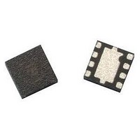
ATF-521P8-TR1 Avago Technologies US Inc., ATF-521P8-TR1 Datasheet - Page 20

ATF-521P8-TR1
Manufacturer Part Number
ATF-521P8-TR1
Description
IC PHEMT 2GHZ 4.5V 200MA 8-LPCC
Manufacturer
Avago Technologies US Inc.
Datasheet
1.ATF-521P8-BLK.pdf
(23 pages)
Specifications of ATF-521P8-TR1
Gain
17dB
Transistor Type
pHEMT FET
Frequency
2GHz
Voltage - Rated
7V
Current Rating
500mA
Noise Figure
1.5dB
Current - Test
200mA
Voltage - Test
4.5V
Power - Output
26.5dBm
Package / Case
8-LPCC
Power Dissipation Pd
1.5W
Rf Transistor Case
LPCC
No. Of Pins
8
Frequency Max
6GHz
Noise Figure Typ
1.5dB
Frequency Min
50MHz
Continuous Drain Current Id
14.8µA
Configuration
Single Dual Source
Drain-gate Voltage (max)
-5 to 1V
Operating Temperature (max)
150C
Operating Temperature Classification
Military
Mounting
Surface Mount
Drain Current Idss Max
200mA
Drain Source Voltage Vds
4.5V
Rohs Compliant
Yes
Lead Free Status / RoHS Status
Lead free / RoHS Compliant
Lead Free Status / RoHS Status
Lead free / RoHS Compliant, Lead free / RoHS Compliant
Available stocks
Company
Part Number
Manufacturer
Quantity
Price
Company:
Part Number:
ATF-521P8-TR1
Manufacturer:
AVAGO
Quantity:
12 367
Company:
Part Number:
ATF-521P8-TR1
Manufacturer:
LATTICE
Quantity:
9
Part Number:
ATF-521P8-TR1
Manufacturer:
AGILENT
Quantity:
20 000
Company:
Part Number:
ATF-521P8-TR1G
Manufacturer:
AVAGO
Quantity:
10 000
Part Number:
ATF-521P8-TR1G
Manufacturer:
AVAGO/安华高
Quantity:
20 000
Using the 3GPP standards document Release 1999
version 2002‑6, the following channel configuration
was used to test ACLR. This table contains the power
levels of the main channels used for Test Model 1.
Note that the DPCH can be made up of 16, 32, or 64
separate channels each at different power levels and
timing offsets. For a listing of power levels, channeliza‑
tion codes and timing offset see the entire 3GPP TS
25.141 V3.10.0 (2002‑06) standards document at: http://
www.3gpp.org/specs/specs.htm
Table 3. ACLR Channel Power Configuration.
3GPP TS 25.141 V3.10.0 (2002-06) Type
P‑CCPCH+SCH
Primary CPICH
PICH
S‑CCPCH containing PCH (SF=256)
DPCH‑64ch (SF=128)
Thermal Design
When working with medium to high power FET
devices, thermal dissipation should be a large part
of the design. This is done to ensure that for a given
ambient temperature the transistor’s channel does not
exceed the maximum rating, T
For example, ATF‑521P8 has a maximum channel tem‑
perature of 150°C and a channel to board thermal
resistance of 45°C/W, thus the entire thermal design
hinges from these key data points. The question that
must be answered is whether this device can operate
in a typical environment with ambient temperature
fluctuations from ‑25°C to 85°C. From Figure 19, a very
useful equation is derived to calculate the temperature
of the channel for a given ambient temperature. These
calculations are all incorporated into Avago Technolo‑
gies AppCAD.
Figure 19. Equivalent Circuit for Thermal Resistance.
Hence very similar to Ohms Law, the temperature of the
channel is calculated with equation 8 below.
T
If no heat sink is used or heat sinking is incorporated
into the PCB board then equation 8 may be reduced to:
T
20
CH
CH
= P
= P
diss
diss
(θ
(θ
ch–b
ch–b
θ
θ
θ
ch-b
b-s
s-a
+ θ
+ θ
b–a
b–s
of the part)
Tb (board
(channel)
) + T
+ θ
Ts (sink)
Ta ( ambient )
or belly
Tch
s–a
amb
) + T
(9)
amb
CH
, on the data sheet.
Pwr (dB)
‑10
‑10
‑18
‑18
‑1.1
(8)
where,
θ
θ
The board to ambient thermal resistance thus becomes
very important for this is the designer’s major source
of heat control. To demonstrate the influence of θ
thermal resistance is measured for two very different
scenarios using the ATF‑521P8 demoboard. The first
case is done with just the demoboard by itself. The
second case is the ATF demoboard mounted on a
chassis or metal casing, and the results are given below:
Table 4. Thermal resistance measurements.
ATF Demoboard
PCB 1/8" Chassis
PCB no HeatSink
Therefore calculating the temperature of the channel
for these two scenarios gives a good indication of what
type of heat sinking is needed.
Case 1: Chassis Mounted @ 85°C
Tch = P x (θ
Tch = 135°C
Case 2: No Heatsink @ 85°C
Tch = P x (θ
Tch = 155°C
In other words, if the board is mounted to a chassis, the
channel temperature is guaranteed to be 135°C safely
below the 150°C maximum. But on the other hand, if
no heat sinking is used and the θ
(32.9°C/W in this case), then the power must be derated
enough to lower the temperature below 150°C. This can
be better understood with Figure 20 below. Note power
is derated at 13 mW/°C for the board with no heat sink
and no derating is required for the chassis mounted
board until an ambient temperature of 100°C.
Pdiss
Figure 20. Derating for ATF- 521P8.
0.9W
(W)
b –a
ch–b
=.9W x (45+32.9)°C/W + 85°C
=.9W x (45+10.4)°C/W +85°C
is the board to ambient thermal resistance;
0
is the channel to board thermal resistance.
ch‑b
ch‑b
81
+ θ
+ θ
100
b‑a
b‑a
) + Ta
) + Ta
θ
10.4°C/W
32.9°C/W
150
Mounted on Chassis
(18 mW/°C)
b-a
No Heatsink
(13 mW/°C)
Tamb ( °C )
b‑a
is above 27°C/W
b‑a,


