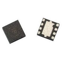
ATF-521P8-TR1 Avago Technologies US Inc., ATF-521P8-TR1 Datasheet - Page 2

ATF-521P8-TR1
Manufacturer Part Number
ATF-521P8-TR1
Description
IC PHEMT 2GHZ 4.5V 200MA 8-LPCC
Manufacturer
Avago Technologies US Inc.
Datasheet
1.ATF-521P8-BLK.pdf
(23 pages)
Specifications of ATF-521P8-TR1
Gain
17dB
Transistor Type
pHEMT FET
Frequency
2GHz
Voltage - Rated
7V
Current Rating
500mA
Noise Figure
1.5dB
Current - Test
200mA
Voltage - Test
4.5V
Power - Output
26.5dBm
Package / Case
8-LPCC
Power Dissipation Pd
1.5W
Rf Transistor Case
LPCC
No. Of Pins
8
Frequency Max
6GHz
Noise Figure Typ
1.5dB
Frequency Min
50MHz
Continuous Drain Current Id
14.8µA
Configuration
Single Dual Source
Drain-gate Voltage (max)
-5 to 1V
Operating Temperature (max)
150C
Operating Temperature Classification
Military
Mounting
Surface Mount
Drain Current Idss Max
200mA
Drain Source Voltage Vds
4.5V
Rohs Compliant
Yes
Lead Free Status / RoHS Status
Lead free / RoHS Compliant
Lead Free Status / RoHS Status
Lead free / RoHS Compliant, Lead free / RoHS Compliant
Available stocks
Company
Part Number
Manufacturer
Quantity
Price
Company:
Part Number:
ATF-521P8-TR1
Manufacturer:
AVAGO
Quantity:
12 367
Company:
Part Number:
ATF-521P8-TR1
Manufacturer:
LATTICE
Quantity:
9
Part Number:
ATF-521P8-TR1
Manufacturer:
AGILENT
Quantity:
20 000
Company:
Part Number:
ATF-521P8-TR1G
Manufacturer:
AVAGO
Quantity:
10 000
Part Number:
ATF-521P8-TR1G
Manufacturer:
AVAGO/安华高
Quantity:
20 000
ATF-521P8 Absolute Maximum Ratings
I
I
P
P
T
T
Notes:
1. Operation of this device in excess of any one of these parameters may cause permanent damage.
2. Assumes DC quiescent conditions.
3. Board (package belly) temperatureT
4. Channel to board thermal resistance measured using 150°C Liquid Crystal Measurement method.
5. Device can safely handle +27dBm RF Input Power provided IGS is limited to 46mA. IGS at P1dB drive level is bias circuit dependent.
Product Consistency Distribution Charts
Notes:
5. Distribution data sample size is 500 samples taken from 5 different wafers. Future wafers allocated to this product may have nominal values
6. Measurements are made on production test board, which represents a trade‑off between optimal OIP3, P1dB and VSWR. Circuit losses have
2
180
150
120
Symbol
V
V
V
θ
DS
GS
Figure 4. Gain @ 2 GHz, 4.5 V, 200 mA.
Nominal = 17.2 dB, LSL = 15.5 dB,
USL = 18.5 dB.
90
60
30
CH
diss
in max.
STG
ch_b
DS
GS
GD
0
Figure 1. Typical I-V Curves.
(V
anywhere between the upper and lower limits.
been de‑embedded from actual measurements.
15
600
500
400
300
200
100
GS
0
= 0.1 V per step)
0
16
2
-3 Std
GAIN (dB)
Parameter
Drain – Source Voltage
Gate –Source Voltage
Gate Drain Voltage
Drain Current
Gate Current
Total Power Dissipation
RF Input Power
Channel Temperature
Storage Temperature
Thermal Resistance
17
V
DS
4
(V)
Vgs = 0.6V
Cpk = 2.13
Stdev = 0.21
+3 Std
18
0.8V
0.7V
0.5V
0.4V
[2]
6
B
[2]
19
[4]
is 25°C. Derate 22 mW/°C for T
[2]
8
[2]
[1]
[3]
[5, 6]
300
250
200
150
100
180
150
120
Figure 5. P1dB @ 2 GHz, 4.5 V, 200 mA.
Nominal = 26.5 dBm, LSL = 25 dBm.
50
Figure 2. NF @ 2 GHz, 4.5 V, 200 mA.
Nominal = 1.5 dB.
90
60
30
0
0
25
0
0.5
25.5
-3 Std
1
P1dB (dBm)
26
-3 Std
NF (dB)
B
> 83°C.
1.5
26.5
Units
mA
mA
W
dBm
°C
°C
°C/W
V
V
V
Cpk = 4.6
Stdev = 0.11
Stdev = 0.19
+3 Std
+3 Std
2
27
2.5
27.5
3
150
120
Figure 3. OIP3 @ 2 GHz, 4.5 V, 200 mA.
Nominal = 41.9 dBm, LSL = 38.5 dBm.
90
60
30
0
37
7
‑5 to 1
‑5 to 1
500
46
1.5
27
150
‑65 to 150
45
Absolute
Maximum
-3 Std
39
41
OIP3 (dBm)
43
45
Cpk = 0.86
Stdev = 1.32
+3 Std
47
49


