ATF-521P8-TR1 Avago Technologies US Inc., ATF-521P8-TR1 Datasheet - Page 16
ATF-521P8-TR1
Manufacturer Part Number
ATF-521P8-TR1
Description
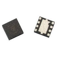
IC PHEMT 2GHZ 4.5V 200MA 8-LPCC
Manufacturer
Avago Technologies US Inc.
Datasheet
1.ATF-521P8-BLK.pdf
(23 pages)
Specifications of ATF-521P8-TR1
Gain
17dB
Transistor Type
pHEMT FET
Frequency
2GHz
Voltage - Rated
7V
Current Rating
500mA
Noise Figure
1.5dB
Current - Test
200mA
Voltage - Test
4.5V
Power - Output
26.5dBm
Package / Case
8-LPCC
Power Dissipation Pd
1.5W
Rf Transistor Case
LPCC
No. Of Pins
8
Frequency Max
6GHz
Noise Figure Typ
1.5dB
Frequency Min
50MHz
Continuous Drain Current Id
14.8µA
Configuration
Single Dual Source
Drain-gate Voltage (max)
-5 to 1V
Operating Temperature (max)
150C
Operating Temperature Classification
Military
Mounting
Surface Mount
Drain Current Idss Max
200mA
Drain Source Voltage Vds
4.5V
Rohs Compliant
Yes
Lead Free Status / RoHS Status
Lead free / RoHS Compliant
Lead Free Status / RoHS Status
Lead free / RoHS Compliant, Lead free / RoHS Compliant
Available stocks
Company
Part Number
Manufacturer
Quantity
Price
Company:

Part Number:
ATF-521P8-TR1
Manufacturer:
AVAGO
Quantity:
12 367
Company:
Part Number:
ATF-521P8-TR1
Manufacturer:
LATTICE
Quantity:
9
Part Number:
ATF-521P8-TR1
Manufacturer:
AGILENT
Quantity:
20 000
Company:
Part Number:
ATF-521P8-TR1G
Manufacturer:
AVAGO
Quantity:
10 000
Part Number:
ATF-521P8-TR1G
Manufacturer:
AVAGO/安华高
Quantity:
20 000


INPUT
Figure 8. Passive Biasing.
Active Bias
Due to very high DC power dissipation and small
package constraints, it is recommended that ATF‑521P8
use active biasing. The main advantage of an active
biasing scheme is the ability to hold the drain to source
current constant over a wide range of temperature
variations.
A very inexpensive method of accomplishing this
is to use two PNP bipolar transistors arranged in a
current mirror configuration as shown in Figure 9. Due
to resistors R1 and R3, this circuit is not acting as a
true current mirror, but if the voltage drop across R1
and R3 is kept identical then it still displays some of
the more useful characteristics of a current mirror. For
example, transistor Q1 is configured with its base and
collector tied together. This acts as a simple PN junction,
which helps temperature compensate the Emitter‑Base
junction of Q2.
RF
Figure 9. Active Bias Circuit.
16
in
Zo
R1
R4
R5
C1
L1
C1
[2]
C3
C2
C4
C3
C2
R2
Q1
I b
R2
R4
L2
R5
V
L4
g
L1
Vdd
C5
C6
R3
Q1
Q2
C4
2
ATF-521P8
2PL
Zo
OUTPUT
V
V
ds
E
R6
L3
7
R3
R1
C8
C5
C7
C6
V
L4
dd
RF
ou t
To calculate the values of R1, R2, R3, and R4 the
following parameters must be know or chosen first:
I
I
V
V
V
V
Q2;
Therefore, resistor R3, which sets the desired device
drain current, is calculated as follows:
R3 = V
where,
I
current and also equal to the reference current I
The next three equations are used to calculate the
rest of the biasing resistors for Figure 9. Note that the
voltage drop across R1 must be set equal to the voltage
drop across R3, but with a current of I
R1 = V
R2 sets the bias current through Q1.
R2 = V
R4 sets the gate voltage for ATF‑521P8.
R4 = V
Thus, by forcing the emitter voltage (V
Q1 equal to V
similar to a current mirror. As long as Q2 operates in the
forward active mode, this holds true. In other words, the
Collector‑Base junction of Q2 must be kept reversed
biased.
ds
R
C2
dd
ds
g
be1
is the Reference current for active bias;
is the device drain‑to‑source current;
is the typical gate bias;
is chosen for stability to be 10 times the typical gate
is the device drain‑to‑source voltage;
is the power supply voltage available;
is the typical Base‑Emitter turn on voltage for Q1 &
I
I
dd
C 2
dd
ds
ds
g
– V
– V
– V
+ I
I
I
R
R
p
C2
be1
ds
ds
ds
p
p
, this circuit regulates the drain current
(7)
(5)
(4)
(6)
R
.
E
) of transistor
R
.
Related parts for ATF-521P8-TR1
Image
Part Number
Description
Manufacturer
Datasheet
Request
R

Part Number:
Description:
IC TRANS E-PHEMT 2GHZ SOT-343
Manufacturer:
Avago Technologies US Inc.
Datasheet:

Part Number:
Description:
IC PHEMT 2GHZ 3V 30MA SOT-343
Manufacturer:
Avago Technologies US Inc.
Datasheet:

Part Number:
Description:
IC PHEMT 2GHZ 2.7V 10MA MINIPAK
Manufacturer:
Avago Technologies US Inc.
Datasheet:

Part Number:
Description:
IC PHEMT 2GHZ 2.7V 10MA SOT-343
Manufacturer:
Avago Technologies US Inc.
Datasheet:
Part Number:
Description:
IC PHEMT 2GHZ 3V 60MA SOT-343
Manufacturer:
Avago Technologies US Inc.
Datasheet:
Part Number:
Description:
IC PHEMT 1.9GHZ 80MA LN SOT-343
Manufacturer:
Avago Technologies US Inc.
Datasheet:
Part Number:
Description:
IC PHEMT 1.9GHZ 15MA LN SOT-343
Manufacturer:
Avago Technologies US Inc.
Part Number:
Description:
IC PHEMT 1.9GHZ 15MA LN SOT-343
Manufacturer:
Avago Technologies US Inc.
Datasheet:
Part Number:
Description:
IC PHEMT 1.9GHZ 60MA LN SOT-343
Manufacturer:
Avago Technologies US Inc.
Datasheet:
Part Number:
Description:
IC TRANS E-PHEMT 2GHZ SOT-343
Manufacturer:
Avago Technologies US Inc.
Datasheet:
Part Number:
Description:
IC TRANS E-PHEMT 2GHZ SOT-343
Manufacturer:
Avago Technologies US Inc.
Datasheet:
Part Number:
Description:
IC TRANS E-PHEMT 2GHZ SOT-343
Manufacturer:
Avago Technologies US Inc.
Datasheet:

Part Number:
Description:
TRANSISTOR,HEMT,N-CHAN,5.5V V(BR)DSS,175mA I(DSS),SOT-343R
Manufacturer:
Avago Technologies US Inc.
Part Number:
Description:
TRANSISTOR,HEMT,N-CHAN,3V V(BR)DSS,15mA I(DSS),SOT-363
Manufacturer:
Avago Technologies US Inc.
Datasheet:
Part Number:
Description:
TRANSISTOR,HEMT,N-CHAN,4.5V V(BR)DSS,90mA I(DSS),SOT-343R
Manufacturer:
Avago Technologies US Inc.
Datasheet: