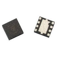
ATF-521P8-TR1 Avago Technologies US Inc., ATF-521P8-TR1 Datasheet - Page 15

ATF-521P8-TR1
Manufacturer Part Number
ATF-521P8-TR1
Description
IC PHEMT 2GHZ 4.5V 200MA 8-LPCC
Manufacturer
Avago Technologies US Inc.
Datasheet
1.ATF-521P8-BLK.pdf
(23 pages)
Specifications of ATF-521P8-TR1
Gain
17dB
Transistor Type
pHEMT FET
Frequency
2GHz
Voltage - Rated
7V
Current Rating
500mA
Noise Figure
1.5dB
Current - Test
200mA
Voltage - Test
4.5V
Power - Output
26.5dBm
Package / Case
8-LPCC
Power Dissipation Pd
1.5W
Rf Transistor Case
LPCC
No. Of Pins
8
Frequency Max
6GHz
Noise Figure Typ
1.5dB
Frequency Min
50MHz
Continuous Drain Current Id
14.8µA
Configuration
Single Dual Source
Drain-gate Voltage (max)
-5 to 1V
Operating Temperature (max)
150C
Operating Temperature Classification
Military
Mounting
Surface Mount
Drain Current Idss Max
200mA
Drain Source Voltage Vds
4.5V
Rohs Compliant
Yes
Lead Free Status / RoHS Status
Lead free / RoHS Compliant
Lead Free Status / RoHS Status
Lead free / RoHS Compliant, Lead free / RoHS Compliant
Available stocks
Company
Part Number
Manufacturer
Quantity
Price
Company:
Part Number:
ATF-521P8-TR1
Manufacturer:
AVAGO
Quantity:
12 367
Company:
Part Number:
ATF-521P8-TR1
Manufacturer:
LATTICE
Quantity:
9
Part Number:
ATF-521P8-TR1
Manufacturer:
AGILENT
Quantity:
20 000
Company:
Part Number:
ATF-521P8-TR1G
Manufacturer:
AVAGO
Quantity:
10 000
Part Number:
ATF-521P8-TR1G
Manufacturer:
AVAGO/安华高
Quantity:
20 000
Amp
Figure 4. High Pass Frequency Response.
The second solution is a low pass configuration with a
shunt capacitor and a series inductor shown in Figure 5
and 6.
RF
Figure 5. Low Pass Circuit Topology.
Amp
Figure 6. Low Pass Frequency Response.
The actual values of these components may be calcu‑
lated by hand on a Smith Chart or more accurately done
on simulation software such as ADS. There are some
advantages and disadvantages of choosing a high pass
versus a low pass. For instance, a high pass circuit
cuts off low frequency gain, which narrows the usable
bandwidth of the amplifier, but consequently helps
avoid potential low frequency instability problems.
A low pass match offers a much broader frequency
response, but it has two major disadvantages. First it has
the potential for low frequency instability, and second it
creates the need for an extra DC blocking capacitor on
the input in order to isolate the device gate from the
preceding stages.
Amp
Figure 7. Input and Output Match for ATF-521P8 at 2 GHz.
15
in
Input Match
L1
C1
Frequency
RF in
RF
Frequency
Frequency
ou t
C1
+
Amp
ATF-521P8
C2
Frequency
Zo
+
Amp
52
Output Match
Frequency
Zo
=
Amp
Figure 7 displays the input and output matching
selected for ATF‑521P8. In this example the input and
output match both essentially function as high pass
filters, but the high frequency gain of the device rolls off
precipitously giving a narrow band frequency response,
yet still wide enough to accommodate a CDMA or
WCDMA transmit band. For more information on RF
matching techniques refer to MGA‑53543 application
note.
Passive Bias
Once the RF matching has been established, the next
step is to DC bias the device. A passive biasing example
is shown in Figure 8. In this example the voltage drop
across resistor R3 sets the drain current (Id) and is calcu‑
lated by the following equation:
R3 = V
where,
V
V
I
I
A voltage divider network with R1 and R2 establishes
the typical gate bias voltage (Vg).
R1 = V
R2 = (V
Often the series resistor, R4, is added to enhance the
low frequency stability. The complete passive bias
example may be found in reference [1].
C3
ds
bb
dd
ds
is the device drain to source current;
for DC stability is 10X the typical gate current;
is the device drain to source voltage;
is the power supply voltage;
Total Response
I
bb
I
g
dd
ds
Frequency
dd
p
+ I
– V
L1
– V
[1]
RF out
bb
V
ds
g
g
) x R1
p
(2)
(3)
(1)


