ATF-521P8-TR1 Avago Technologies US Inc., ATF-521P8-TR1 Datasheet - Page 17
ATF-521P8-TR1
Manufacturer Part Number
ATF-521P8-TR1
Description
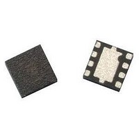
IC PHEMT 2GHZ 4.5V 200MA 8-LPCC
Manufacturer
Avago Technologies US Inc.
Datasheet
1.ATF-521P8-BLK.pdf
(23 pages)
Specifications of ATF-521P8-TR1
Gain
17dB
Transistor Type
pHEMT FET
Frequency
2GHz
Voltage - Rated
7V
Current Rating
500mA
Noise Figure
1.5dB
Current - Test
200mA
Voltage - Test
4.5V
Power - Output
26.5dBm
Package / Case
8-LPCC
Power Dissipation Pd
1.5W
Rf Transistor Case
LPCC
No. Of Pins
8
Frequency Max
6GHz
Noise Figure Typ
1.5dB
Frequency Min
50MHz
Continuous Drain Current Id
14.8µA
Configuration
Single Dual Source
Drain-gate Voltage (max)
-5 to 1V
Operating Temperature (max)
150C
Operating Temperature Classification
Military
Mounting
Surface Mount
Drain Current Idss Max
200mA
Drain Source Voltage Vds
4.5V
Rohs Compliant
Yes
Lead Free Status / RoHS Status
Lead free / RoHS Compliant
Lead Free Status / RoHS Status
Lead free / RoHS Compliant, Lead free / RoHS Compliant
Available stocks
Company
Part Number
Manufacturer
Quantity
Price
Company:

Part Number:
ATF-521P8-TR1
Manufacturer:
AVAGO
Quantity:
12 367
Company:
Part Number:
ATF-521P8-TR1
Manufacturer:
LATTICE
Quantity:
9
Part Number:
ATF-521P8-TR1
Manufacturer:
AGILENT
Quantity:
20 000
Company:
Part Number:
ATF-521P8-TR1G
Manufacturer:
AVAGO
Quantity:
10 000
Part Number:
ATF-521P8-TR1G
Manufacturer:
AVAGO/安华高
Quantity:
20 000


PCB Layout
A recommended PCB pad layout for the Leadless Plastic
Chip Carrier (LPCC) package used by the ATF‑521P8 is
shown in Figure 10. This layout provides plenty of plated
through hole vias for good thermal and RF grounding. It
also provides a good transition from microstrip to the
device package. For more detailed dimensions refer to
Section 9 of the data sheet.
Figure 10. Microstripline Layout.
RF Grounding
Unlike SOT packages, ATF‑521P8 is housed in a leadless
package with the die mounted directly to the lead
frame or the belly of the package shown in Figure 11.
Figure 11. LPCC Package for ATF-521P8.
Figure 12. ATF-521P8 demoboard.
17
Pin 7 (Drain)
Pin 8
Pin 6
Pin 5
Bottom View
J1
Pin 1 (Source)
Pin 2 (Gate)
Pin 3
Pin 4 (Source)
C1
C4
C3
R4
R2
short
L1
0
R1
R3
C6
C7
C5
C8
J2
This simplifies RF grounding by reducing the amount
of inductance from the source to ground. It is also
recommended to ground pins 1 and 4 since they are
also connected to the device source. Pins 3, 5, 6, and 8
are not connected, but may be used to help dissipate
heat from the package or for better alignment when
soldering the device.
This three‑layer board (Figure 12) contains a 10‑mil layer
and a 52‑mil layer separated by a ground plane. The first
layer is Getek RG200D material with dielectric constant
of 3.8. The second layer is for mechanical rigidity and
consists of FR4 with dielectric constant of 4.2.
High Linearity Tx Driver
The need for higher data rates and increased voice
capacity gave rise to a new third generation standard
know as Wideband CDMA or UMTS. This new standard
requires higher performance from radio components
such as higher dynamic range and better linearity. For
example, a WCDMA waveform has a very high peak to
average ratio which forces amplifiers in a transmit chain
to have very good Adjacent Channel Leakage power
Ratio or ACLR, or else operate in a backed off mode.
If the amplifier is not backed off then the waveform is
compressed and the signal becomes very nonlinear.
This application example presents a highly linear
transmit drive for use in the 2.14GHz frequency range.
Using the RF matching techniques described earlier,
ATF‑521P8 is matched to the following input and output
impedances:
Related parts for ATF-521P8-TR1
Image
Part Number
Description
Manufacturer
Datasheet
Request
R

Part Number:
Description:
IC TRANS E-PHEMT 2GHZ SOT-343
Manufacturer:
Avago Technologies US Inc.
Datasheet:

Part Number:
Description:
IC PHEMT 2GHZ 3V 30MA SOT-343
Manufacturer:
Avago Technologies US Inc.
Datasheet:

Part Number:
Description:
IC PHEMT 2GHZ 2.7V 10MA MINIPAK
Manufacturer:
Avago Technologies US Inc.
Datasheet:

Part Number:
Description:
IC PHEMT 2GHZ 2.7V 10MA SOT-343
Manufacturer:
Avago Technologies US Inc.
Datasheet:
Part Number:
Description:
IC PHEMT 2GHZ 3V 60MA SOT-343
Manufacturer:
Avago Technologies US Inc.
Datasheet:
Part Number:
Description:
IC PHEMT 1.9GHZ 80MA LN SOT-343
Manufacturer:
Avago Technologies US Inc.
Datasheet:
Part Number:
Description:
IC PHEMT 1.9GHZ 15MA LN SOT-343
Manufacturer:
Avago Technologies US Inc.
Part Number:
Description:
IC PHEMT 1.9GHZ 15MA LN SOT-343
Manufacturer:
Avago Technologies US Inc.
Datasheet:
Part Number:
Description:
IC PHEMT 1.9GHZ 60MA LN SOT-343
Manufacturer:
Avago Technologies US Inc.
Datasheet:
Part Number:
Description:
IC TRANS E-PHEMT 2GHZ SOT-343
Manufacturer:
Avago Technologies US Inc.
Datasheet:
Part Number:
Description:
IC TRANS E-PHEMT 2GHZ SOT-343
Manufacturer:
Avago Technologies US Inc.
Datasheet:
Part Number:
Description:
IC TRANS E-PHEMT 2GHZ SOT-343
Manufacturer:
Avago Technologies US Inc.
Datasheet:

Part Number:
Description:
TRANSISTOR,HEMT,N-CHAN,5.5V V(BR)DSS,175mA I(DSS),SOT-343R
Manufacturer:
Avago Technologies US Inc.
Part Number:
Description:
TRANSISTOR,HEMT,N-CHAN,3V V(BR)DSS,15mA I(DSS),SOT-363
Manufacturer:
Avago Technologies US Inc.
Datasheet:
Part Number:
Description:
TRANSISTOR,HEMT,N-CHAN,4.5V V(BR)DSS,90mA I(DSS),SOT-343R
Manufacturer:
Avago Technologies US Inc.
Datasheet: