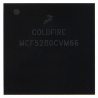
MCF5280CVM66 Freescale Semiconductor, MCF5280CVM66 Datasheet - Page 375

MCF5280CVM66
Manufacturer Part Number
MCF5280CVM66
Description
IC MPU 32BIT COLDF 256-MAPBGA
Manufacturer
Freescale Semiconductor
Series
MCF528xr
Datasheet
1.MCF5216CVM66J.pdf
(766 pages)
Specifications of MCF5280CVM66
Core Processor
Coldfire V2
Core Size
32-Bit
Speed
66MHz
Connectivity
CAN, EBI/EMI, Ethernet, I²C, SPI, UART/USART
Peripherals
DMA, LVD, POR, PWM, WDT
Number Of I /o
142
Program Memory Type
ROMless
Ram Size
64K x 8
Voltage - Supply (vcc/vdd)
2.7 V ~ 3.6 V
Data Converters
A/D 8x10b
Oscillator Type
External
Operating Temperature
-40°C ~ 85°C
Package / Case
256-MAPBGA
Controller Family/series
ColdFire
No. Of I/o's
150
Program Memory Size
2KB
Ram Memory Size
64KB
Cpu Speed
66.67MHz
Embedded Interface Type
CAN, I2C, SPI, UART
No. Of Pwm Channels
8
Rohs Compliant
Yes
Lead Free Status / RoHS Status
Lead free / RoHS Compliant
Eeprom Size
-
Program Memory Size
-
Available stocks
Company
Part Number
Manufacturer
Quantity
Price
Company:
Part Number:
MCF5280CVM66
Manufacturer:
FREESCAL
Quantity:
151
Company:
Part Number:
MCF5280CVM66
Manufacturer:
Freescale Semiconductor
Quantity:
10 000
Company:
Part Number:
MCF5280CVM66J
Manufacturer:
Freescale Semiconductor
Quantity:
10 000
Company:
Part Number:
MCF5280CVM66L
Manufacturer:
FREESCAL
Quantity:
151
- Current page: 375 of 766
- Download datasheet (9Mb)
20.5.4
20.5.5
Freescale Semiconductor
Bit(s)
Bit(s)
7–4
3–0
7–4
3–0
Address
GPT Output Compare 3 Data Register (GPTOC3D)
GPT Counter Register (GPTCNT)
Reset
Field
R/W
Address
A successful channel 3 output compare overrides any channel 2:0 compares.
For each OC3M bit that is set, the output compare action reflects the
corresponding OC3D bit.
Reset
Field
R/W
15
OC3M
Name
Name
OC3D
—
—
Figure 20-5. GPT Output Compare 3 Data Register (GPTOC3D)
MCF5282 and MCF5216 ColdFire Microcontroller User’s Manual, Rev. 3
7
Reserved, should be cleared.
Output compare 3 mask. Setting an OC3M bit configures the corresponding PORTTn
pin to be an output. OC3Mn makes the GPT port pin an output regardless of the data
direction bit when the pin is configured for output compare (IOSx = 1). The OC3Mn
bits do not change the state of the PORTTnDDR bits. These bits are read anytime,
write anytime.
1 Corresponding PORTTn pin configured as output
0 No effect
Reserved, should be cleared.
Output compare 3 data. When a successful channel 3 output compare occurs, these
bits transfer to the PORTTn data register if the corresponding OC3Mn bits are set.
These bits are read anytime, write anytime.
Figure 20-6. GPT Counter Register (GPTCNT)
Table 20-6. GPTOC3M Field Descriptions
Table 20-7. GPTOC3D Field Descriptions
—
IPSBAR + 0x1A_0004, 0x1B_0004
IPSBAR + 0x1A_0003, 0x1B_0003
0000_0000_0000_0000
NOTE
0000_0000
Read only
4
CNTR
R/W
Description
3
Description
General Purpose Timer Modules (GPTA and GPTB)
OC3D
0
0
20-7
Related parts for MCF5280CVM66
Image
Part Number
Description
Manufacturer
Datasheet
Request
R
Part Number:
Description:
Manufacturer:
Freescale Semiconductor, Inc
Datasheet:
Part Number:
Description:
Manufacturer:
Freescale Semiconductor, Inc
Datasheet:
Part Number:
Description:
Manufacturer:
Freescale Semiconductor, Inc
Datasheet:
Part Number:
Description:
Manufacturer:
Freescale Semiconductor, Inc
Datasheet:
Part Number:
Description:
Manufacturer:
Freescale Semiconductor, Inc
Datasheet:
Part Number:
Description:
Manufacturer:
Freescale Semiconductor, Inc
Datasheet:
Part Number:
Description:
Manufacturer:
Freescale Semiconductor, Inc
Datasheet:
Part Number:
Description:
Manufacturer:
Freescale Semiconductor, Inc
Datasheet:
Part Number:
Description:
Manufacturer:
Freescale Semiconductor, Inc
Datasheet:
Part Number:
Description:
Manufacturer:
Freescale Semiconductor, Inc
Datasheet:
Part Number:
Description:
Manufacturer:
Freescale Semiconductor, Inc
Datasheet:
Part Number:
Description:
Manufacturer:
Freescale Semiconductor, Inc
Datasheet:
Part Number:
Description:
Manufacturer:
Freescale Semiconductor, Inc
Datasheet:
Part Number:
Description:
Manufacturer:
Freescale Semiconductor, Inc
Datasheet:
Part Number:
Description:
Manufacturer:
Freescale Semiconductor, Inc
Datasheet:


