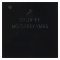
MCF5280CVM66 Freescale Semiconductor, MCF5280CVM66 Datasheet - Page 294

MCF5280CVM66
Manufacturer Part Number
MCF5280CVM66
Description
IC MPU 32BIT COLDF 256-MAPBGA
Manufacturer
Freescale Semiconductor
Series
MCF528xr
Datasheet
1.MCF5216CVM66J.pdf
(766 pages)
Specifications of MCF5280CVM66
Core Processor
Coldfire V2
Core Size
32-Bit
Speed
66MHz
Connectivity
CAN, EBI/EMI, Ethernet, I²C, SPI, UART/USART
Peripherals
DMA, LVD, POR, PWM, WDT
Number Of I /o
142
Program Memory Type
ROMless
Ram Size
64K x 8
Voltage - Supply (vcc/vdd)
2.7 V ~ 3.6 V
Data Converters
A/D 8x10b
Oscillator Type
External
Operating Temperature
-40°C ~ 85°C
Package / Case
256-MAPBGA
Controller Family/series
ColdFire
No. Of I/o's
150
Program Memory Size
2KB
Ram Memory Size
64KB
Cpu Speed
66.67MHz
Embedded Interface Type
CAN, I2C, SPI, UART
No. Of Pwm Channels
8
Rohs Compliant
Yes
Lead Free Status / RoHS Status
Lead free / RoHS Compliant
Eeprom Size
-
Program Memory Size
-
Available stocks
Company
Part Number
Manufacturer
Quantity
Price
Company:
Part Number:
MCF5280CVM66
Manufacturer:
FREESCAL
Quantity:
151
Company:
Part Number:
MCF5280CVM66
Manufacturer:
Freescale Semiconductor
Quantity:
10 000
Company:
Part Number:
MCF5280CVM66J
Manufacturer:
Freescale Semiconductor
Quantity:
10 000
Company:
Part Number:
MCF5280CVM66L
Manufacturer:
FREESCAL
Quantity:
151
- Current page: 294 of 766
- Download datasheet (9Mb)
Synchronous DRAM Controller Module
15.3.4
Again, in this example only the second 512-Kbyte block of each 1-Mbyte space is accessed in each bank.
In addition, the SDRAM component is mapped only to readable and writable supervisor and user data. The
DMRs have the following configuration.
With this configuration, the DMR0 = 0x0074_0075, as described in
15-22
31–18
17–16
15–9
Bits
Setting
Setting
8
7
6
5
4
3
2
1
0
(hex)
(hex)
Field
Field
DMR Initialization
Name
BAM
WP
AM
SC
SD
UC
UD
C/I
—
—
—
V
Bits
31
15
2–0
3
Setting
0
1
1
1
0
1
0
1
Name
IP
—
MCF5282 and MCF5216 ColdFire Microcontroller User’s Manual, Rev. 3
With bits 17 and 16 as don’t cares, BAM = 0x0074, which leaves bank select bits and upper
512K select bits unmasked. Note that bits 22 and 21 are set because they are used as bank
selects; bit 20 is set because it controls the 1-Mbyte boundary address.
Reserved. Don’t care.
Reserved. Don’t care.
Allow reads and writes
Reserved. Don’t care.
Disable CPU space access.
Disable alternate master access.
Disable supervisor code accesses.
Enable supervisor data accesses.
Disable user code accesses.
Enable user data accesses.
Enable accesses.
Table 15-28. DACR Initialization Values (continued)
—
Setting
Table 15-29. DMR0 Initialization Values
0
Figure 15-14. DMR0 Register
Indicates precharge has not been initiated.
Reserved. Don’t care.
0000_0000_0111_01xx
xxxx_xxx0_x111_0101
9
BAM
WP
8
0 074
0075
—
Description
7
Description
C/I
6
Table
AM
5
15-29.
SC
4
SD
3
Freescale Semiconductor
UC
18
2
UD
17
1
—
16
V
0
Related parts for MCF5280CVM66
Image
Part Number
Description
Manufacturer
Datasheet
Request
R
Part Number:
Description:
Manufacturer:
Freescale Semiconductor, Inc
Datasheet:
Part Number:
Description:
Manufacturer:
Freescale Semiconductor, Inc
Datasheet:
Part Number:
Description:
Manufacturer:
Freescale Semiconductor, Inc
Datasheet:
Part Number:
Description:
Manufacturer:
Freescale Semiconductor, Inc
Datasheet:
Part Number:
Description:
Manufacturer:
Freescale Semiconductor, Inc
Datasheet:
Part Number:
Description:
Manufacturer:
Freescale Semiconductor, Inc
Datasheet:
Part Number:
Description:
Manufacturer:
Freescale Semiconductor, Inc
Datasheet:
Part Number:
Description:
Manufacturer:
Freescale Semiconductor, Inc
Datasheet:
Part Number:
Description:
Manufacturer:
Freescale Semiconductor, Inc
Datasheet:
Part Number:
Description:
Manufacturer:
Freescale Semiconductor, Inc
Datasheet:
Part Number:
Description:
Manufacturer:
Freescale Semiconductor, Inc
Datasheet:
Part Number:
Description:
Manufacturer:
Freescale Semiconductor, Inc
Datasheet:
Part Number:
Description:
Manufacturer:
Freescale Semiconductor, Inc
Datasheet:
Part Number:
Description:
Manufacturer:
Freescale Semiconductor, Inc
Datasheet:
Part Number:
Description:
Manufacturer:
Freescale Semiconductor, Inc
Datasheet:


